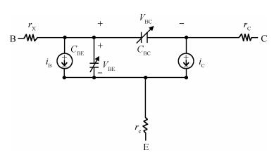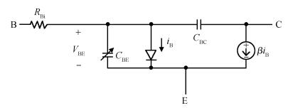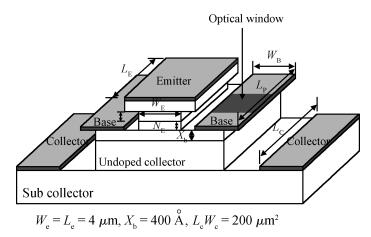
Fig. 1.
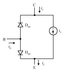
T model for bipolar transistor.
SEMICONDUCTOR DEVICES
Hassan Kaatuzian, Hadi Dehghan Nayeri, Masoud Ataei and Ashkan Zandi
Corresponding author: Hassan Kaatuzian, Email: hsnkato@aut.ac.ir
Abstract: We analyze an integrated electrically pumped opto-electronic mixer, which consists of two InP/GaInAs hetero junction bipolar transistors (HBT), in a cascode configuration. A new HBT with modified physical structure is proposed and simulated to improve the frequency characteristics of a cascode mixer. For the verification and calibrating software simulator, we compare the simulation results of a typical HBT, before modifying it and comparing it with empirical reported experiments. Then we examine the simulator on our modified proposed HBT to prove its wider frequency characteristics with better flatness and acceptable down conversion gain. Although the idea is examined in several GHz modulation, it may easily be extended to state of the art HBT cascode mixers in much higher frequency range.
Keywords: cascode, down conversion gain, mixer, opto-electronic, photo HBT, simulation
| [1] |
Darcie T. Sub carrier multiplexing for multiple-access light wave networks. J Lightwave Technol, 1987, 5(8):1103 doi: 10.1109/JLT.1987.1075615
|
| [2] |
Liu C P, Seeds A J, Wake D. Two-terminal edge-coupled InP/InGaAs heterojunction phototransistor optoelectronic mixer. IEEE Microw Guided Wave Lett, 1997, 7(3):72 doi: 10.1109/75.556036
|
| [3] |
Betser Y, Lasri J, Sidorov V, et al. An integrated heterojunction bipolar transistor cascode opto-electronic mixer. IEEE Trans Microw Theory Tech, 1999, 47(7):1358 doi: 10.1109/22.775479
|
| [4] |
Sedra A S, Smith K C. Microelectronic circuits. USA:Oxford University Press, 1997
|
| [5] |
Liu W. Fundamentals of Ⅲ-Ⅴ devices. USA:John Wiley and Sons, 1999
|
| [6] |
Chandrasekhar S, Luanardi L M, Gnauck A H, et al. High-speed monolithic pin/HBT and HPT/HBT photoreceivers implemented with simple phototransistor structure. IEEE Photonics Technol Lett, 1993, 5(11):1316 doi: 10.1109/68.250055
|
| [7] |
Betser Y, Ritter D. A single-stage three-terminal heterojunction bipolar transistor optoelectronic mixer. J Lightwave Technol, 1998, 16(4):605 doi: 10.1109/50.664070
|
| [8] |
Hamm R A, Ritter D, Temkin H. A compact MOMBE growth system. J Vac Sci Technol, 1997, A12:2790 http://depa.fquim.unam.mx/amyd/archivero/VITEK_17603.pdf
|
| [9] |
Kaatuzian H, Nayeri H D. Characteristics improvement of an integrated HBT cascode opto-electronic mixer. AOE Conference Proceedings SaK43. pdf, China, 2008
|
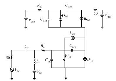
Table 1. Values of the equivalent circuit components.

|
Table 2. Set of physical dimensions for our new proposed HBT device.

|
Table 3. Comparison between some equivalent circuit components in this work and Ref. [3].

|
| [1] |
Darcie T. Sub carrier multiplexing for multiple-access light wave networks. J Lightwave Technol, 1987, 5(8):1103 doi: 10.1109/JLT.1987.1075615
|
| [2] |
Liu C P, Seeds A J, Wake D. Two-terminal edge-coupled InP/InGaAs heterojunction phototransistor optoelectronic mixer. IEEE Microw Guided Wave Lett, 1997, 7(3):72 doi: 10.1109/75.556036
|
| [3] |
Betser Y, Lasri J, Sidorov V, et al. An integrated heterojunction bipolar transistor cascode opto-electronic mixer. IEEE Trans Microw Theory Tech, 1999, 47(7):1358 doi: 10.1109/22.775479
|
| [4] |
Sedra A S, Smith K C. Microelectronic circuits. USA:Oxford University Press, 1997
|
| [5] |
Liu W. Fundamentals of Ⅲ-Ⅴ devices. USA:John Wiley and Sons, 1999
|
| [6] |
Chandrasekhar S, Luanardi L M, Gnauck A H, et al. High-speed monolithic pin/HBT and HPT/HBT photoreceivers implemented with simple phototransistor structure. IEEE Photonics Technol Lett, 1993, 5(11):1316 doi: 10.1109/68.250055
|
| [7] |
Betser Y, Ritter D. A single-stage three-terminal heterojunction bipolar transistor optoelectronic mixer. J Lightwave Technol, 1998, 16(4):605 doi: 10.1109/50.664070
|
| [8] |
Hamm R A, Ritter D, Temkin H. A compact MOMBE growth system. J Vac Sci Technol, 1997, A12:2790 http://depa.fquim.unam.mx/amyd/archivero/VITEK_17603.pdf
|
| [9] |
Kaatuzian H, Nayeri H D. Characteristics improvement of an integrated HBT cascode opto-electronic mixer. AOE Conference Proceedings SaK43. pdf, China, 2008
|


Article views: 5034 Times PDF downloads: 12 Times Cited by: 0 Times
Received: 13 February 2013 Revised: 17 March 2013 Online: Published: 01 September 2013
| Citation: |
Hassan Kaatuzian, Hadi Dehghan Nayeri, Masoud Ataei, Ashkan Zandi. Structural parameters improvement of an integrated HBT in a cascode configuration opto-electronic mixer[J]. Journal of Semiconductors, 2013, 34(9): 094001. doi: 10.1088/1674-4926/34/9/094001
****
H Kaatuzian, H D Nayeri, M Ataei, A Zandi. Structural parameters improvement of an integrated HBT in a cascode configuration opto-electronic mixer[J]. J. Semicond., 2013, 34(9): 094001. doi: 10.1088/1674-4926/34/9/094001.

|
| [1] |
Darcie T. Sub carrier multiplexing for multiple-access light wave networks. J Lightwave Technol, 1987, 5(8):1103 doi: 10.1109/JLT.1987.1075615
|
| [2] |
Liu C P, Seeds A J, Wake D. Two-terminal edge-coupled InP/InGaAs heterojunction phototransistor optoelectronic mixer. IEEE Microw Guided Wave Lett, 1997, 7(3):72 doi: 10.1109/75.556036
|
| [3] |
Betser Y, Lasri J, Sidorov V, et al. An integrated heterojunction bipolar transistor cascode opto-electronic mixer. IEEE Trans Microw Theory Tech, 1999, 47(7):1358 doi: 10.1109/22.775479
|
| [4] |
Sedra A S, Smith K C. Microelectronic circuits. USA:Oxford University Press, 1997
|
| [5] |
Liu W. Fundamentals of Ⅲ-Ⅴ devices. USA:John Wiley and Sons, 1999
|
| [6] |
Chandrasekhar S, Luanardi L M, Gnauck A H, et al. High-speed monolithic pin/HBT and HPT/HBT photoreceivers implemented with simple phototransistor structure. IEEE Photonics Technol Lett, 1993, 5(11):1316 doi: 10.1109/68.250055
|
| [7] |
Betser Y, Ritter D. A single-stage three-terminal heterojunction bipolar transistor optoelectronic mixer. J Lightwave Technol, 1998, 16(4):605 doi: 10.1109/50.664070
|
| [8] |
Hamm R A, Ritter D, Temkin H. A compact MOMBE growth system. J Vac Sci Technol, 1997, A12:2790 http://depa.fquim.unam.mx/amyd/archivero/VITEK_17603.pdf
|
| [9] |
Kaatuzian H, Nayeri H D. Characteristics improvement of an integrated HBT cascode opto-electronic mixer. AOE Conference Proceedings SaK43. pdf, China, 2008
|

 WeChat ID
Journal of Semiconductors © 2017 All Rights Reserved 京ICP备05085259号-2

 DownLoad: