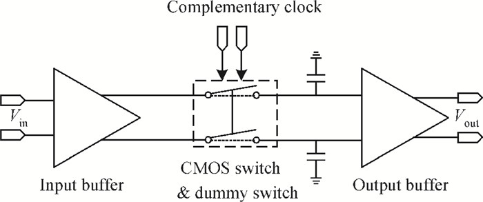
Fig. 1.
Block diagram of the THA.
SEMICONDUCTOR INTEGRATED CIRCUITS
Kai Tang1, 2, Qiao Meng1, 2, , Zhigong Wang1, 2, Yi Zhang1, 2, Kuai Yin1, 2 and Ting Guo1, 2
Corresponding author: Meng Qiao, Email:mengqiao@seu.edu.cn
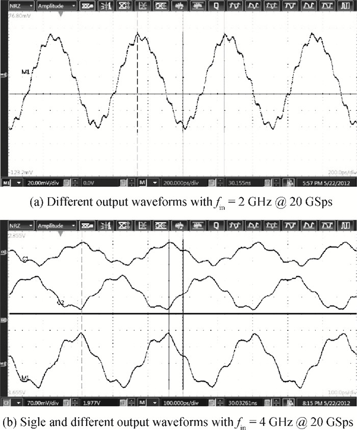
Abstract: An open-loop 20 GSps track-and-hold amplifier (THA) using fully-differential architecture to mitigate common-mode noise and suppress even-order harmonics is presented. CMOS switch and dummy switches are adopted to achieve high speed and good linearity. A cross-coupled pair is used in the input buffer to suppress the charge injection and clock feedthrough. Both the input and output buffers use an active inductor load to achieve high signal bandwidth. The THA is realized with 0.18 μm SiGe BiCMOS technology using only CMOS devices at a 1.8 V voltage supply and with a core area of 0.024 mm2. The measurement results show that the SFDR is 32.4 dB with a 4 GHz sine wave input at a 20 GSps sampling rate, and the third harmonic distortion is -48 dBc. The effective resolution bandwidth of the THA is 12 GHz and the figure of merit is only 0.028 mW/GHz.
Keywords: track-and-hold amplifier (THA), ADC, ultra-high-speed, SiGe BiCMOS, low power
| [1] |
Li X, Kuo W M L, Cressler J D. A 40 GS/s SiGe track-and-hold amplifier. IEEE BCTM 1.1, 2008:1 http://ieeexplore.ieee.org/document/4662699/
|
| [2] |
Lu Y, Kuo W M L, Li X, et al. An 8-bit, 12 GSample/sec SiGe track-and-hold amplifier. Proc BCTM, 2005:148 http://ieeexplore.ieee.org/document/1555221/?arnumber=1555221&punumber%3D10419
|
| [3] |
Lee J, Baeyens Y, Weiner J, et al. A 50 GS/S distributed T/H amplifier in 0.18μm SiGe BiCMOS. IEEE ISSCC, 2007:466
|
| [4] |
Orser H, Gopinath A. A 20GS/s 1.2 V 0.13μm CMOS switched cascode track-and-hold amplifier. IEEE Trans Circuits Syst Ⅱ:Express Briefs, 2010, 57(7):512 doi: 10.1109/TCSII.2010.2048484
|
| [5] |
Li X, Kuo W L, Lu Y, et al. A 5-bit, 18 GS/sec SiGe HBT track-and-hold amplifier. IEEE CSICS, 2005:105 http://ieeexplore.ieee.org/document/1531774/?arnumber=1531774&sortType%3Dasc_p_Sequence%26filter%3DAND(p_IS_Number:32673)%26rowsPerPage%3D100
|
| [6] |
Yamanaka S, Sano K, Murata K. A 20-Gs/s track-and-hold amplifier in InP HBT technology. IEEE Trans Microw Theory Tech, 2010, 58(9):2334 doi: 10.1109/TMTT.2010.2057174
|
| [7] |
Borokhovych Y, Gustat H, Tillack B, et al. A low-power, 10 Gs/s track-and-hold amplifier in SiGe BiCMOS technology. Proceedings of ESSCIRC, Grenoble, France, 2005:263 doi: 10.1088/1674-4926/34/9/095002/meta;jsessionid=F5EDDE583483386A095E13CF00FF6F27.ip-10-40-2-120
|
| [8] |
Tang K, Meng Q. A 20 GSps track-and-hold circuit in 90 nm CMOS technology. IEEE Proceeding of ICATC, 2012:237 doi: 10.1088/1674-4926/34/9/095002/meta
|
| [9] |
Wang I H, Liu S I. A 4-bit, 13.5 G Sample/sec track-and-hold circuit. VLSI Design, Automation and Test, 2007:1
|
| [10] |
Han L, Liu X, Bai T, et al. A 2.5 Gb/s CMOS low noise transimpedance amplifier with active feedback. Research & Progress of Solid State Electronics, 2008, 28(3):415 http://en.cnki.com.cn/Article_en/CJFDTOTAL-GTDZ200803023.htm
|
| [11] |
Fayomi C J B, Roberts G W, Sawan M. Low-voltage CMOS analog bootstrapped switch for sample-and-hold circuit:design and chip characterization. Proceedings of the IEEE ISCAS, Kobe, 2005, 23:2200
|
| [12] |
Jakonis D, Svenson C. A 1 GHz linearized CMOS track and hold circuit. Proceedings of the IEEE ISCAS, Arizona, 2002, 5:597 http://www.diva-portal.org/smash/record.jsf?pid=diva2%3A255694&dswid=9804
|
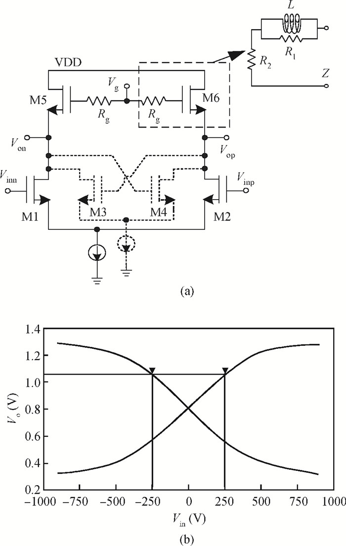
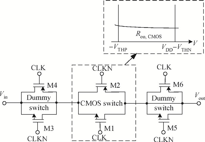
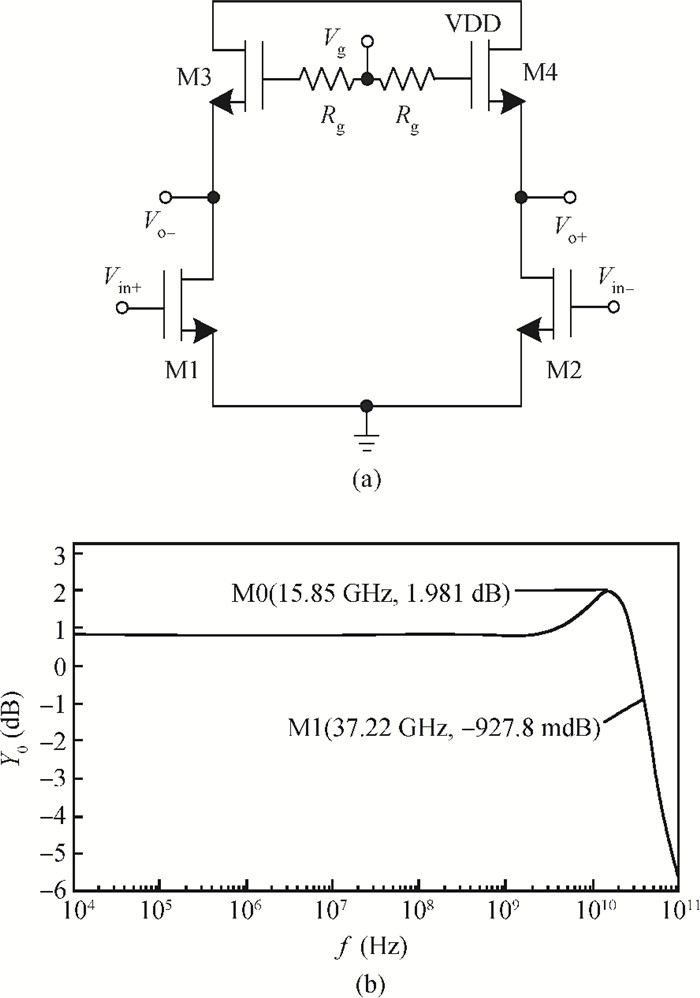
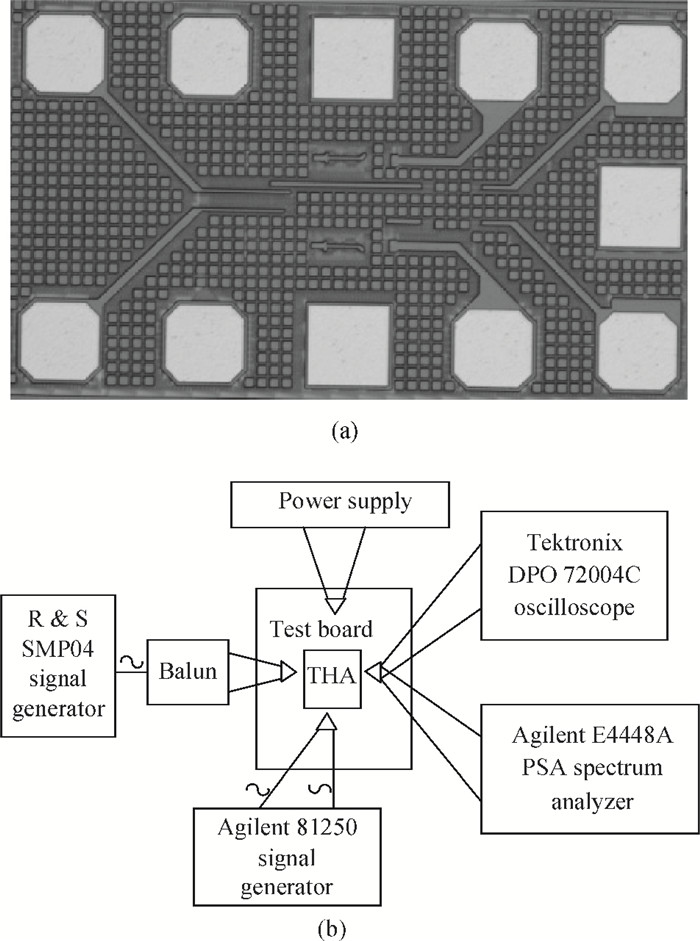

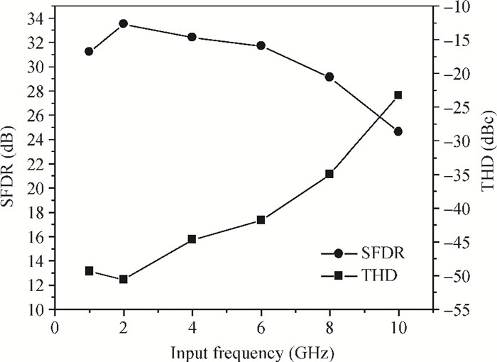
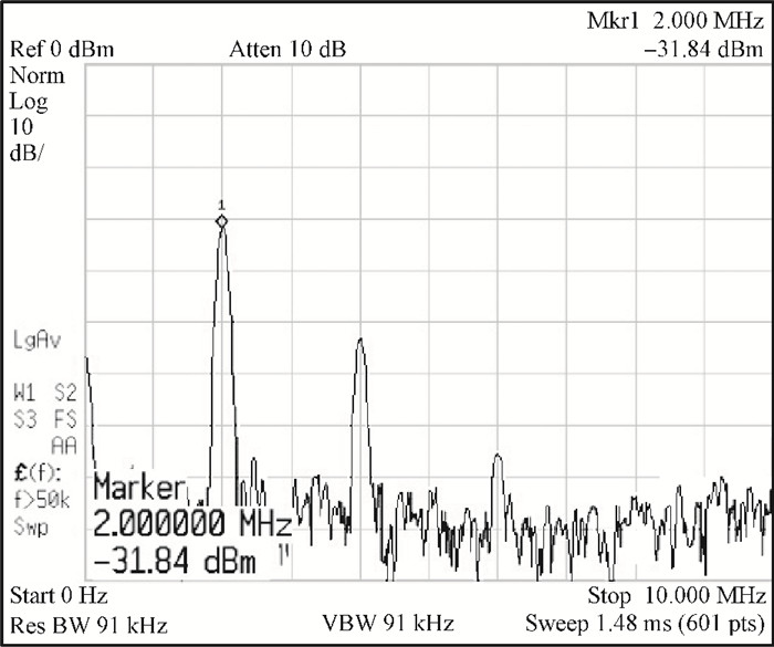
Table 1. Performance summary and comparison.

|
| [1] |
Li X, Kuo W M L, Cressler J D. A 40 GS/s SiGe track-and-hold amplifier. IEEE BCTM 1.1, 2008:1 http://ieeexplore.ieee.org/document/4662699/
|
| [2] |
Lu Y, Kuo W M L, Li X, et al. An 8-bit, 12 GSample/sec SiGe track-and-hold amplifier. Proc BCTM, 2005:148 http://ieeexplore.ieee.org/document/1555221/?arnumber=1555221&punumber%3D10419
|
| [3] |
Lee J, Baeyens Y, Weiner J, et al. A 50 GS/S distributed T/H amplifier in 0.18μm SiGe BiCMOS. IEEE ISSCC, 2007:466
|
| [4] |
Orser H, Gopinath A. A 20GS/s 1.2 V 0.13μm CMOS switched cascode track-and-hold amplifier. IEEE Trans Circuits Syst Ⅱ:Express Briefs, 2010, 57(7):512 doi: 10.1109/TCSII.2010.2048484
|
| [5] |
Li X, Kuo W L, Lu Y, et al. A 5-bit, 18 GS/sec SiGe HBT track-and-hold amplifier. IEEE CSICS, 2005:105 http://ieeexplore.ieee.org/document/1531774/?arnumber=1531774&sortType%3Dasc_p_Sequence%26filter%3DAND(p_IS_Number:32673)%26rowsPerPage%3D100
|
| [6] |
Yamanaka S, Sano K, Murata K. A 20-Gs/s track-and-hold amplifier in InP HBT technology. IEEE Trans Microw Theory Tech, 2010, 58(9):2334 doi: 10.1109/TMTT.2010.2057174
|
| [7] |
Borokhovych Y, Gustat H, Tillack B, et al. A low-power, 10 Gs/s track-and-hold amplifier in SiGe BiCMOS technology. Proceedings of ESSCIRC, Grenoble, France, 2005:263 doi: 10.1088/1674-4926/34/9/095002/meta;jsessionid=F5EDDE583483386A095E13CF00FF6F27.ip-10-40-2-120
|
| [8] |
Tang K, Meng Q. A 20 GSps track-and-hold circuit in 90 nm CMOS technology. IEEE Proceeding of ICATC, 2012:237 doi: 10.1088/1674-4926/34/9/095002/meta
|
| [9] |
Wang I H, Liu S I. A 4-bit, 13.5 G Sample/sec track-and-hold circuit. VLSI Design, Automation and Test, 2007:1
|
| [10] |
Han L, Liu X, Bai T, et al. A 2.5 Gb/s CMOS low noise transimpedance amplifier with active feedback. Research & Progress of Solid State Electronics, 2008, 28(3):415 http://en.cnki.com.cn/Article_en/CJFDTOTAL-GTDZ200803023.htm
|
| [11] |
Fayomi C J B, Roberts G W, Sawan M. Low-voltage CMOS analog bootstrapped switch for sample-and-hold circuit:design and chip characterization. Proceedings of the IEEE ISCAS, Kobe, 2005, 23:2200
|
| [12] |
Jakonis D, Svenson C. A 1 GHz linearized CMOS track and hold circuit. Proceedings of the IEEE ISCAS, Arizona, 2002, 5:597 http://www.diva-portal.org/smash/record.jsf?pid=diva2%3A255694&dswid=9804
|


Article views: 3324 Times PDF downloads: 18 Times Cited by: 0 Times
Received: 21 February 2013 Revised: 03 April 2013 Online: Published: 01 September 2013
| Citation: |
Kai Tang, Qiao Meng, Zhigong Wang, Yi Zhang, Kuai Yin, Ting Guo. A low-power 20 GSps track-and-hold amplifier in 0.18 μm SiGe BiCMOS technology[J]. Journal of Semiconductors, 2013, 34(9): 095002. doi: 10.1088/1674-4926/34/9/095002
****
K Tang, Q Meng, Z G Wang, Y Zhang, K Yin, T Guo. A low-power 20 GSps track-and-hold amplifier in 0.18 μm SiGe BiCMOS technology[J]. J. Semicond., 2013, 34(9): 095002. doi: 10.1088/1674-4926/34/9/095002.

|
| [1] |
Li X, Kuo W M L, Cressler J D. A 40 GS/s SiGe track-and-hold amplifier. IEEE BCTM 1.1, 2008:1 http://ieeexplore.ieee.org/document/4662699/
|
| [2] |
Lu Y, Kuo W M L, Li X, et al. An 8-bit, 12 GSample/sec SiGe track-and-hold amplifier. Proc BCTM, 2005:148 http://ieeexplore.ieee.org/document/1555221/?arnumber=1555221&punumber%3D10419
|
| [3] |
Lee J, Baeyens Y, Weiner J, et al. A 50 GS/S distributed T/H amplifier in 0.18μm SiGe BiCMOS. IEEE ISSCC, 2007:466
|
| [4] |
Orser H, Gopinath A. A 20GS/s 1.2 V 0.13μm CMOS switched cascode track-and-hold amplifier. IEEE Trans Circuits Syst Ⅱ:Express Briefs, 2010, 57(7):512 doi: 10.1109/TCSII.2010.2048484
|
| [5] |
Li X, Kuo W L, Lu Y, et al. A 5-bit, 18 GS/sec SiGe HBT track-and-hold amplifier. IEEE CSICS, 2005:105 http://ieeexplore.ieee.org/document/1531774/?arnumber=1531774&sortType%3Dasc_p_Sequence%26filter%3DAND(p_IS_Number:32673)%26rowsPerPage%3D100
|
| [6] |
Yamanaka S, Sano K, Murata K. A 20-Gs/s track-and-hold amplifier in InP HBT technology. IEEE Trans Microw Theory Tech, 2010, 58(9):2334 doi: 10.1109/TMTT.2010.2057174
|
| [7] |
Borokhovych Y, Gustat H, Tillack B, et al. A low-power, 10 Gs/s track-and-hold amplifier in SiGe BiCMOS technology. Proceedings of ESSCIRC, Grenoble, France, 2005:263 doi: 10.1088/1674-4926/34/9/095002/meta;jsessionid=F5EDDE583483386A095E13CF00FF6F27.ip-10-40-2-120
|
| [8] |
Tang K, Meng Q. A 20 GSps track-and-hold circuit in 90 nm CMOS technology. IEEE Proceeding of ICATC, 2012:237 doi: 10.1088/1674-4926/34/9/095002/meta
|
| [9] |
Wang I H, Liu S I. A 4-bit, 13.5 G Sample/sec track-and-hold circuit. VLSI Design, Automation and Test, 2007:1
|
| [10] |
Han L, Liu X, Bai T, et al. A 2.5 Gb/s CMOS low noise transimpedance amplifier with active feedback. Research & Progress of Solid State Electronics, 2008, 28(3):415 http://en.cnki.com.cn/Article_en/CJFDTOTAL-GTDZ200803023.htm
|
| [11] |
Fayomi C J B, Roberts G W, Sawan M. Low-voltage CMOS analog bootstrapped switch for sample-and-hold circuit:design and chip characterization. Proceedings of the IEEE ISCAS, Kobe, 2005, 23:2200
|
| [12] |
Jakonis D, Svenson C. A 1 GHz linearized CMOS track and hold circuit. Proceedings of the IEEE ISCAS, Arizona, 2002, 5:597 http://www.diva-portal.org/smash/record.jsf?pid=diva2%3A255694&dswid=9804
|

 WeChat ID
Journal of Semiconductors © 2017 All Rights Reserved 京ICP备05085259号-2

 DownLoad: