Fig. 1.
Progress cross section of InP DHBTs technology.
SEMICONDUCTOR INTEGRATED CIRCUITS
Hongfei Yao, Xiantai Wang, Danyu Wu, Yongbo Su, Yuxiong Cao, Ji Ge, Xiaoxi Ning and Zhi Jin
Corresponding author: Jin Zhi, Email:jinzhi@ime.ac.cn
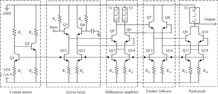
Abstract: A W-band frequency doubler MMIC is designed and fabricated using 1-μm InP DHBT technology. Active balun is employed to transform the single-ended signal into differential output. Push-push configuration loaded with harmonic resonant network is utilized to acquire the second harmonic frequency. A multi-stage differential structure improves the conversion gain and suppresses the fundamental frequency. The MMIC occupies an area of 0.55×0.5 mm2 with 18 DHBTs integrated. Measurements show that the output power is above 5.8 dBm with the suppression of fundamental frequency below -16 dBc and the conversion gain above 4.7 dB over 75-80 GHz.
Keywords: frequency doubler, W-band, InP, DHBT, push-push
| [1] |
Puyal V, Konczykowska A, Nouet P. DC-100-GHz frequency doublers in InP DHBT technology. IEEE Trans Microw Theory Tech, 2005, 53(4):1338 doi: 10.1109/TMTT.2005.845766
|
| [2] |
An D W, Yu W H, Lv X. Design and analysis of a 2 mm-band tripler based on quartz. J Infrared Millim Wave, 2011, 30(4):377
|
| [3] |
Yang T, Xiang X J, Wu W. Broad-band tripler of W-band. J Infrared Millim Wave, 2007, 26(3):161 http://en.cnki.com.cn/Article_en/CJFDTOTAL-HWYH200703000.htm
|
| [4] |
Jin Z, Su Y B, Cheng W. High current multi-finger InGaAs/InP double heterojunction bipolar transistor with the maximum oscillation frequency 253 GHz. Chin Phys Lett, 2008, 25(8):3075 doi: 10.1088/0256-307X/25/8/091
|
| [5] |
Cheng W, Jin Z, Yu J Y. Design of InGaAsP composite collector for InP DHBT. Chinese Journal of Semiconductors, 2007, 28(6):131 doi: 10.1143/JJAP.43.2243/pdf; jsessionid=8799A660736756D1964EA3A7687F8640.c3.iopscience.cld.iop.org
|
| [6] |
Cao Y X, Jin Z, Ge J. A symbolically defined InP double heterojunction bipolar transistor large-signal model. Journal of Semiconductors, 2009, 30(12):37 http://www.jos.ac.cn/bdtxbcn/ch/reader/view_abstract.aspx?file_no=09060503&flag=1
|
| [7] |
Kobayashi K W, OKI A K, Tran L T. A 108-GHz InP-HBT monolithic push-push VCO with low phase noise and wide tuning bandwidth. IEEE J Solid-State Circuits, 1999, 34(9):1225 doi: 10.1109/4.782080
|
| [8] |
Li Q, Wang Z G, Li W. Design of 20-44 GHz broadband doubler MMIC. Journal of Semiconductors, 2010, 31(4):045012 doi: 10.1088/1674-4926/31/4/045012
|
| [9] |
Maas S A. Nonlinear microwave and RF circuits. Norwood, MA:Artech House, 2003 http://ci.nii.ac.jp/ncid/BA63628377
|
| [10] |
Hung J J, Hancock T M, Rebeiz G M. High-power high-efficiency SiGe Ku-and Ka-band balanced frequency doublers. IEEE Trans Microw Theory Tech, 2005, 53(2):754 doi: 10.1109/TMTT.2004.840615
|
| [11] |
Campos-Roca Y, Verweyen L, Fernández-Barciela M. 38/76 GHz PHEMT MMIC balanced frequency doublers in coplanar technology. IEEE Microw Wireless Compon Lett, 2000, 10(11):484 http://cat.inist.fr/?aModele=afficheN&cpsidt=819389
|
| [12] |
Liu G, Ulusoy A C, Trasser A. 60-80 GHz frequency doubler operating close to fmax. APMC, 2010:770
|
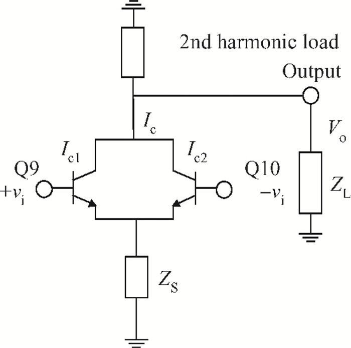

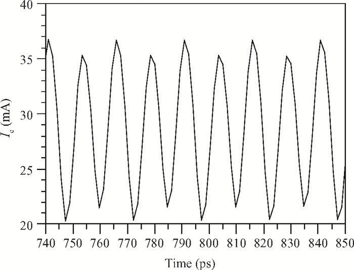
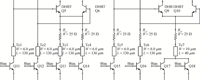
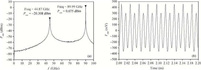
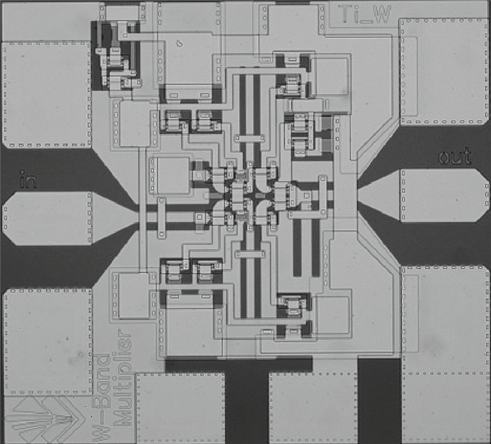


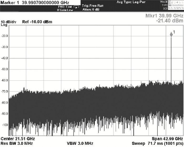
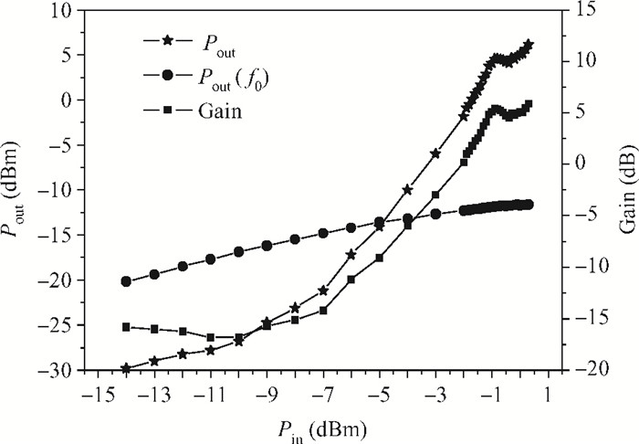
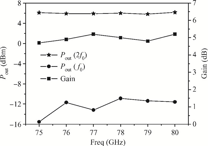
Table 1. Performance summary and comparison.

|
| [1] |
Puyal V, Konczykowska A, Nouet P. DC-100-GHz frequency doublers in InP DHBT technology. IEEE Trans Microw Theory Tech, 2005, 53(4):1338 doi: 10.1109/TMTT.2005.845766
|
| [2] |
An D W, Yu W H, Lv X. Design and analysis of a 2 mm-band tripler based on quartz. J Infrared Millim Wave, 2011, 30(4):377
|
| [3] |
Yang T, Xiang X J, Wu W. Broad-band tripler of W-band. J Infrared Millim Wave, 2007, 26(3):161 http://en.cnki.com.cn/Article_en/CJFDTOTAL-HWYH200703000.htm
|
| [4] |
Jin Z, Su Y B, Cheng W. High current multi-finger InGaAs/InP double heterojunction bipolar transistor with the maximum oscillation frequency 253 GHz. Chin Phys Lett, 2008, 25(8):3075 doi: 10.1088/0256-307X/25/8/091
|
| [5] |
Cheng W, Jin Z, Yu J Y. Design of InGaAsP composite collector for InP DHBT. Chinese Journal of Semiconductors, 2007, 28(6):131 doi: 10.1143/JJAP.43.2243/pdf; jsessionid=8799A660736756D1964EA3A7687F8640.c3.iopscience.cld.iop.org
|
| [6] |
Cao Y X, Jin Z, Ge J. A symbolically defined InP double heterojunction bipolar transistor large-signal model. Journal of Semiconductors, 2009, 30(12):37 http://www.jos.ac.cn/bdtxbcn/ch/reader/view_abstract.aspx?file_no=09060503&flag=1
|
| [7] |
Kobayashi K W, OKI A K, Tran L T. A 108-GHz InP-HBT monolithic push-push VCO with low phase noise and wide tuning bandwidth. IEEE J Solid-State Circuits, 1999, 34(9):1225 doi: 10.1109/4.782080
|
| [8] |
Li Q, Wang Z G, Li W. Design of 20-44 GHz broadband doubler MMIC. Journal of Semiconductors, 2010, 31(4):045012 doi: 10.1088/1674-4926/31/4/045012
|
| [9] |
Maas S A. Nonlinear microwave and RF circuits. Norwood, MA:Artech House, 2003 http://ci.nii.ac.jp/ncid/BA63628377
|
| [10] |
Hung J J, Hancock T M, Rebeiz G M. High-power high-efficiency SiGe Ku-and Ka-band balanced frequency doublers. IEEE Trans Microw Theory Tech, 2005, 53(2):754 doi: 10.1109/TMTT.2004.840615
|
| [11] |
Campos-Roca Y, Verweyen L, Fernández-Barciela M. 38/76 GHz PHEMT MMIC balanced frequency doublers in coplanar technology. IEEE Microw Wireless Compon Lett, 2000, 10(11):484 http://cat.inist.fr/?aModele=afficheN&cpsidt=819389
|
| [12] |
Liu G, Ulusoy A C, Trasser A. 60-80 GHz frequency doubler operating close to fmax. APMC, 2010:770
|


Article views: 4174 Times PDF downloads: 40 Times Cited by: 0 Times
Received: 06 February 2013 Revised: 26 March 2013 Online: Published: 01 September 2013
| Citation: |
Hongfei Yao, Xiantai Wang, Danyu Wu, Yongbo Su, Yuxiong Cao, Ji Ge, Xiaoxi Ning, Zhi Jin. W-band push-push monolithic frequency doubler in 1-μm InP DHBT technology[J]. Journal of Semiconductors, 2013, 34(9): 095006. doi: 10.1088/1674-4926/34/9/095006
****
H F Yao, X T Wang, D Y Wu, Y B Su, Y X Cao, J Ge, X X Ning, Z Jin. W-band push-push monolithic frequency doubler in 1-μm InP DHBT technology[J]. J. Semicond., 2013, 34(9): 095006. doi: 10.1088/1674-4926/34/9/095006.

|
| [1] |
Puyal V, Konczykowska A, Nouet P. DC-100-GHz frequency doublers in InP DHBT technology. IEEE Trans Microw Theory Tech, 2005, 53(4):1338 doi: 10.1109/TMTT.2005.845766
|
| [2] |
An D W, Yu W H, Lv X. Design and analysis of a 2 mm-band tripler based on quartz. J Infrared Millim Wave, 2011, 30(4):377
|
| [3] |
Yang T, Xiang X J, Wu W. Broad-band tripler of W-band. J Infrared Millim Wave, 2007, 26(3):161 http://en.cnki.com.cn/Article_en/CJFDTOTAL-HWYH200703000.htm
|
| [4] |
Jin Z, Su Y B, Cheng W. High current multi-finger InGaAs/InP double heterojunction bipolar transistor with the maximum oscillation frequency 253 GHz. Chin Phys Lett, 2008, 25(8):3075 doi: 10.1088/0256-307X/25/8/091
|
| [5] |
Cheng W, Jin Z, Yu J Y. Design of InGaAsP composite collector for InP DHBT. Chinese Journal of Semiconductors, 2007, 28(6):131 doi: 10.1143/JJAP.43.2243/pdf; jsessionid=8799A660736756D1964EA3A7687F8640.c3.iopscience.cld.iop.org
|
| [6] |
Cao Y X, Jin Z, Ge J. A symbolically defined InP double heterojunction bipolar transistor large-signal model. Journal of Semiconductors, 2009, 30(12):37 http://www.jos.ac.cn/bdtxbcn/ch/reader/view_abstract.aspx?file_no=09060503&flag=1
|
| [7] |
Kobayashi K W, OKI A K, Tran L T. A 108-GHz InP-HBT monolithic push-push VCO with low phase noise and wide tuning bandwidth. IEEE J Solid-State Circuits, 1999, 34(9):1225 doi: 10.1109/4.782080
|
| [8] |
Li Q, Wang Z G, Li W. Design of 20-44 GHz broadband doubler MMIC. Journal of Semiconductors, 2010, 31(4):045012 doi: 10.1088/1674-4926/31/4/045012
|
| [9] |
Maas S A. Nonlinear microwave and RF circuits. Norwood, MA:Artech House, 2003 http://ci.nii.ac.jp/ncid/BA63628377
|
| [10] |
Hung J J, Hancock T M, Rebeiz G M. High-power high-efficiency SiGe Ku-and Ka-band balanced frequency doublers. IEEE Trans Microw Theory Tech, 2005, 53(2):754 doi: 10.1109/TMTT.2004.840615
|
| [11] |
Campos-Roca Y, Verweyen L, Fernández-Barciela M. 38/76 GHz PHEMT MMIC balanced frequency doublers in coplanar technology. IEEE Microw Wireless Compon Lett, 2000, 10(11):484 http://cat.inist.fr/?aModele=afficheN&cpsidt=819389
|
| [12] |
Liu G, Ulusoy A C, Trasser A. 60-80 GHz frequency doubler operating close to fmax. APMC, 2010:770
|

 WeChat ID
Journal of Semiconductors © 2017 All Rights Reserved 京ICP备05085259号-2

 DownLoad: