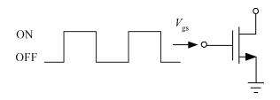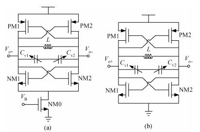
Fig. 1.
Conventional LC VCOs. (a) With tail current source. (b) Without tail current source
SEMICONDUCTOR INTEGRATED CIRCUITS
Nan Chen, Shengxi Diao, Lu Huang, Xuefei Bai and Fujiang Lin
Corresponding author: Diao Shengxi, Email:diaosxi@ustc.edu.cn
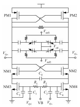
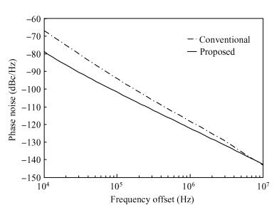
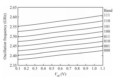
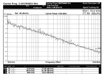
Abstract: To meet the requirements of the low power Zigbee system, VCO design optimizations of phase noise, power consumption and frequency tuning are discussed in this paper. Both flicker noise of tail bias transistors and up-conversion of flicker noise from cross-coupled pair are reduced by improved self-switched biasing technology, leading to low close-in phase noise. Low power is achieved by low supply voltage and triode region biasing. To linearly tune the frequency and get constant gain, distributed varactor structure is adopted. The proposed VCO is fabricated in SMIC 0.18-μm CMOS process. The measured linear tuning range is from 2.38 to 2.61 GHz. The oscillator exhibits low phase noise of -77.5 dBc/Hz and -122.8 dBc/Hz at 10 kHz and 1 MHz offset, respectively, at 2.55 GHz oscillation frequency while dissipating 2.7 mA from 1.2 V supply voltage, which well meet design specifications.
Keywords: VCO, flicker noise, tuning characteristics, low power
| [1] |
Hegazi E, Sjoland H, Abidi A A. A filtering technique to lower LC oscillator phase noise. IEEE J Solid-State Circuits, 2001, 36(12):1921 doi: 10.1109/4.972142
|
| [2] |
Bloom I, Nemirovsky Y. 1/f noise reduction of metal-oxide-semiconductor transistors by cycling from inversion to accumulation. Appl Phys Lett, 1991, 58(15):1664 doi: 10.1063/1.105130
|
| [3] |
Klumperink E A M, Gierkink S L J, Wel A P, et al. Reducing MOSFET 1/f noise and power consumption by switched biasing. IEEE J Solid-State Circuits, 2000, 35(7):994 doi: 10.1109/4.848208
|
| [4] |
Boon C C, Do M A, Yeo K S, et al. RF CMOS low-phase-noise LC oscillator through memory reduction tail transistor. IEEE Trans Circuits Syst Ⅱ:Express Briefs, 2004, 51(2):85 doi: 10.1109/TCSII.2003.821519
|
| [5] |
Huang G H, Kim B S. Low phase noise self-switched biasing LC quadrature VCO. IEEE Trans Microw Theory Tech, 2009, 57(2):344 doi: 10.1109/TMTT.2008.2009901
|
| [6] |
Hegazi E, Rael J, Abidi A A. The designer's guide to high-purity oscillator. New York:Springer, 2005
|
| [7] |
Jerng A, Sodini C G. The impact of device type and sizing on phase noise mechanisms. IEEE J Solid-State Circuits, 2005, 40(2):360 doi: 10.1109/JSSC.2004.841035
|
| [8] |
Levantino S, Samori C, Zanchi A, et al. AM-to-PM conversion in varactor-tuned oscillators. IEEE Trans Circuits Syst Ⅱ:Express Briefs, 2002, 49(7):509 doi: 10.1109/TCSII.2002.804051
|
| [9] |
Ismail A, Abidi A A. CMOS differential LC oscillator with suppressed up-converted flicker noise. IEEE International Solid State Circuits Conference, 2003:98
|
| [10] |
Mira J, Dival T, Ramet S, et al. Distributed MOS varactor biasing for VCO gain equalization in 0.13μm CMOS technology. IEEE Radio Frequency Integrated Circuits Symposium, 2004:131
|
| [11] |
Young D J, Mallin S J, Cross M. 2 GHz CMOS voltage-controlled oscillator with optimal design of phase noise and power dissipation. IEEE Radio Frequency Integrated Circuits Symposium, 2007:131
|
| [12] |
Park K G, Jeong C Y, Park J W, et al. Current reusing VCO and divide-by-two frequency divider for quadrature LO generation. IEEE Microw Wireless Compon Lett, 2008, 18(6):413 doi: 10.1109/LMWC.2008.922674
|
| [13] |
Hong J P and Lee S G. Gm-boosted differential drain-to-source feedback colpitts CMOS VCO. IEEE Trans Microw Theory Tech, 2011, 59(7):1811 doi: 10.1109/TMTT.2011.2138712
|
| [14] |
Yin X, Ma C Y, Ye T C, et al. A low-phase-noise LC-VCO with an enhanced-Q varactor for use in a high-sensitivity GNSS receiver. Journal of Semiconductors, 2012, 33(5):055002 doi: 10.1088/1674-4926/33/5/055002
|
Table 1. Comparison of performance with prior works

|
| [1] |
Hegazi E, Sjoland H, Abidi A A. A filtering technique to lower LC oscillator phase noise. IEEE J Solid-State Circuits, 2001, 36(12):1921 doi: 10.1109/4.972142
|
| [2] |
Bloom I, Nemirovsky Y. 1/f noise reduction of metal-oxide-semiconductor transistors by cycling from inversion to accumulation. Appl Phys Lett, 1991, 58(15):1664 doi: 10.1063/1.105130
|
| [3] |
Klumperink E A M, Gierkink S L J, Wel A P, et al. Reducing MOSFET 1/f noise and power consumption by switched biasing. IEEE J Solid-State Circuits, 2000, 35(7):994 doi: 10.1109/4.848208
|
| [4] |
Boon C C, Do M A, Yeo K S, et al. RF CMOS low-phase-noise LC oscillator through memory reduction tail transistor. IEEE Trans Circuits Syst Ⅱ:Express Briefs, 2004, 51(2):85 doi: 10.1109/TCSII.2003.821519
|
| [5] |
Huang G H, Kim B S. Low phase noise self-switched biasing LC quadrature VCO. IEEE Trans Microw Theory Tech, 2009, 57(2):344 doi: 10.1109/TMTT.2008.2009901
|
| [6] |
Hegazi E, Rael J, Abidi A A. The designer's guide to high-purity oscillator. New York:Springer, 2005
|
| [7] |
Jerng A, Sodini C G. The impact of device type and sizing on phase noise mechanisms. IEEE J Solid-State Circuits, 2005, 40(2):360 doi: 10.1109/JSSC.2004.841035
|
| [8] |
Levantino S, Samori C, Zanchi A, et al. AM-to-PM conversion in varactor-tuned oscillators. IEEE Trans Circuits Syst Ⅱ:Express Briefs, 2002, 49(7):509 doi: 10.1109/TCSII.2002.804051
|
| [9] |
Ismail A, Abidi A A. CMOS differential LC oscillator with suppressed up-converted flicker noise. IEEE International Solid State Circuits Conference, 2003:98
|
| [10] |
Mira J, Dival T, Ramet S, et al. Distributed MOS varactor biasing for VCO gain equalization in 0.13μm CMOS technology. IEEE Radio Frequency Integrated Circuits Symposium, 2004:131
|
| [11] |
Young D J, Mallin S J, Cross M. 2 GHz CMOS voltage-controlled oscillator with optimal design of phase noise and power dissipation. IEEE Radio Frequency Integrated Circuits Symposium, 2007:131
|
| [12] |
Park K G, Jeong C Y, Park J W, et al. Current reusing VCO and divide-by-two frequency divider for quadrature LO generation. IEEE Microw Wireless Compon Lett, 2008, 18(6):413 doi: 10.1109/LMWC.2008.922674
|
| [13] |
Hong J P and Lee S G. Gm-boosted differential drain-to-source feedback colpitts CMOS VCO. IEEE Trans Microw Theory Tech, 2011, 59(7):1811 doi: 10.1109/TMTT.2011.2138712
|
| [14] |
Yin X, Ma C Y, Ye T C, et al. A low-phase-noise LC-VCO with an enhanced-Q varactor for use in a high-sensitivity GNSS receiver. Journal of Semiconductors, 2012, 33(5):055002 doi: 10.1088/1674-4926/33/5/055002
|


Article views: 3657 Times PDF downloads: 30 Times Cited by: 0 Times
Received: 03 February 2013 Revised: 19 March 2013 Online: Published: 01 September 2013
| Citation: |
Nan Chen, Shengxi Diao, Lu Huang, Xuefei Bai, Fujiang Lin. Design optimizations of phase noise, power consumption and frequency tuning for VCO[J]. Journal of Semiconductors, 2013, 34(9): 095009. doi: 10.1088/1674-4926/34/9/095009
****
N Chen, S X Diao, L Huang, X F Bai, F J Lin. Design optimizations of phase noise, power consumption and frequency tuning for VCO[J]. J. Semicond., 2013, 34(9): 095009. doi: 10.1088/1674-4926/34/9/095009.

|
| [1] |
Hegazi E, Sjoland H, Abidi A A. A filtering technique to lower LC oscillator phase noise. IEEE J Solid-State Circuits, 2001, 36(12):1921 doi: 10.1109/4.972142
|
| [2] |
Bloom I, Nemirovsky Y. 1/f noise reduction of metal-oxide-semiconductor transistors by cycling from inversion to accumulation. Appl Phys Lett, 1991, 58(15):1664 doi: 10.1063/1.105130
|
| [3] |
Klumperink E A M, Gierkink S L J, Wel A P, et al. Reducing MOSFET 1/f noise and power consumption by switched biasing. IEEE J Solid-State Circuits, 2000, 35(7):994 doi: 10.1109/4.848208
|
| [4] |
Boon C C, Do M A, Yeo K S, et al. RF CMOS low-phase-noise LC oscillator through memory reduction tail transistor. IEEE Trans Circuits Syst Ⅱ:Express Briefs, 2004, 51(2):85 doi: 10.1109/TCSII.2003.821519
|
| [5] |
Huang G H, Kim B S. Low phase noise self-switched biasing LC quadrature VCO. IEEE Trans Microw Theory Tech, 2009, 57(2):344 doi: 10.1109/TMTT.2008.2009901
|
| [6] |
Hegazi E, Rael J, Abidi A A. The designer's guide to high-purity oscillator. New York:Springer, 2005
|
| [7] |
Jerng A, Sodini C G. The impact of device type and sizing on phase noise mechanisms. IEEE J Solid-State Circuits, 2005, 40(2):360 doi: 10.1109/JSSC.2004.841035
|
| [8] |
Levantino S, Samori C, Zanchi A, et al. AM-to-PM conversion in varactor-tuned oscillators. IEEE Trans Circuits Syst Ⅱ:Express Briefs, 2002, 49(7):509 doi: 10.1109/TCSII.2002.804051
|
| [9] |
Ismail A, Abidi A A. CMOS differential LC oscillator with suppressed up-converted flicker noise. IEEE International Solid State Circuits Conference, 2003:98
|
| [10] |
Mira J, Dival T, Ramet S, et al. Distributed MOS varactor biasing for VCO gain equalization in 0.13μm CMOS technology. IEEE Radio Frequency Integrated Circuits Symposium, 2004:131
|
| [11] |
Young D J, Mallin S J, Cross M. 2 GHz CMOS voltage-controlled oscillator with optimal design of phase noise and power dissipation. IEEE Radio Frequency Integrated Circuits Symposium, 2007:131
|
| [12] |
Park K G, Jeong C Y, Park J W, et al. Current reusing VCO and divide-by-two frequency divider for quadrature LO generation. IEEE Microw Wireless Compon Lett, 2008, 18(6):413 doi: 10.1109/LMWC.2008.922674
|
| [13] |
Hong J P and Lee S G. Gm-boosted differential drain-to-source feedback colpitts CMOS VCO. IEEE Trans Microw Theory Tech, 2011, 59(7):1811 doi: 10.1109/TMTT.2011.2138712
|
| [14] |
Yin X, Ma C Y, Ye T C, et al. A low-phase-noise LC-VCO with an enhanced-Q varactor for use in a high-sensitivity GNSS receiver. Journal of Semiconductors, 2012, 33(5):055002 doi: 10.1088/1674-4926/33/5/055002
|

 WeChat ID
Journal of Semiconductors © 2017 All Rights Reserved 京ICP备05085259号-2

 DownLoad: