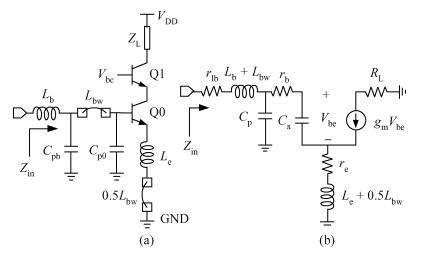
Fig. 1.
(a) LNA topology and (b) simplified small signal equivalent circuit
SEMICONDUCTOR INTEGRATED CIRCUITS
Renjie Zhou1, , Yong Xiang1, Hong Wang1, Yebing Gan2, 3, Min Qian2, 3, Chengyan Ma1, 2, 3 and Tianchun Ye1
Corresponding author: Zhou Renjie, Email:zrjustc@gmail.com
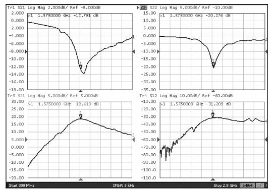
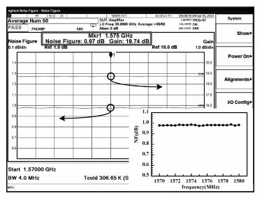
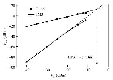
Abstract: A monolithic integrated low noise amplifier (LNA) based on a SiGe HBT process for a global navigation satellite system (GNSS) is presented. An optimizing strategy of taking parasitic capacities at the input node into consideration is adopted and a method and design equations of monolithically designing the LC load and the output impedance matching circuit are introduced. The LNA simultaneously reaches excellent noise and input/output impedance matching. The measurement results show that the LNA gives an ultra-low noise figure of 0.97 dB, a power gain of 18.6 dB and a three-order input intermodulation point of -6 dBm at the frequency of 1.575 GHz. The chip consumes 5.4 mW from a 1.8 V source and occupies 600×650 μm2 die area.
Keywords: LNA, GNSS, monolithic integrated, SiGe HBT
| [1] |
Poh J C H, Cheng P, Thrivikraman T K, et al. High gain, high linearity, L-band SiGe low noise amplifier with fully-integrated matching network. IEEE Topical Meeting on Silicon Monolithic Integrated Circuits in RF Systems (SiRF), 2010:69 http://ieeexplore.ieee.org/abstract/document/5422953/
|
| [2] |
Huang H, Zhang H Y, Yang H, et al. A super-low-noise, high-gain MMIC LNA. Chinese Journal of Semiconductors, 2006, 27(12):2080 http://www.jos.ac.cn/bdtxben/ch/reader/view_abstract.aspx?file_no=06070401&flag=1
|
| [3] |
Li Z Q, Chen L, Zhang H. Design and optimization of CMOS LNA with ESD protection for 2.4 GHz WSN application. Journal of Semiconductors, 2011, 32(10):105004 doi: 10.1088/1674-4926/32/10/105004
|
| [4] |
Lu Z Y, Xie H Y, Huo W J, et al. 0.9 GHz and 2.4 GHz dual-band SiGe HBT LNA. Journal of Semiconductors, 2013, 34(2):025002 doi: 10.1088/1674-4926/34/2/025002
|
| [5] |
Wu C H, Tsai W C, Tan C G, et al. A GPS/Galileo SoC with adaptive in-band blocker cancellation in 65 nm CMOS. IEEE International Solid-State Circuits Conference Digest of Technical Papers (ISSCC), 2011:462 http://ieeexplore.ieee.org/document/5746398/keywords
|
| [6] |
Bergervoet J, Leenaerts D M, De Jong G W, et al. A 1.95 GHz sub-1 dB NF, +40 dBm OIP3 WCDMA LNA module. IEEE J Solid-State Circuits, 2012, 47(7):1672 doi: 10.1109/JSSC.2012.2191673
|
| [7] |
Niehenke E C. The evolution of low noise devices and amplifiers. IEEE MTT-S International Microwave Symposium Digest (MTT), 2012:1 http://ieeexplore.ieee.org/document/6258248/authors
|
| [8] |
Sivonen P, Kangasmaa S, Parssinen A. Analysis of packaging effects and optimization in inductively degenerated common-emitter low-noise amplifiers. IEEE Trans Microw Theory Tech, 2003, 51(4):1220 doi: 10.1109/TMTT.2003.809633
|
| [9] |
Niu G. Noise in SiGe HBT RF technology:physics, modeling, and circuit implications. Proc IEEE, 2005, 93(9):1583 doi: 10.1109/JPROC.2005.852226
|
| [10] |
Li J, Li W Y. A fully integrated LNA for COMPASS receiver in SiGe-BiCMOS technology. IEEE MTT-S InternationalMicrowave Workshop Series on Millimeter Wave Wireless Technology and Applications (IMWS), 2012:1
|
| [11] |
Kang B, Yu J, Shin H, et al. Design and analysis of a cascode bipolar low-noise amplifier with capacitive shunt feedback under power-constraint. IEEE Trans Microw Theory Tech, 2011, 59(6):1539 doi: 10.1109/TMTT.2011.2136355
|
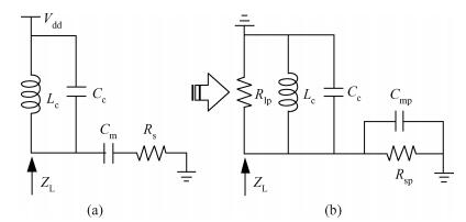
Table 1. Main design parameters

|
Table 2. Performance summary and comparison

|
| [1] |
Poh J C H, Cheng P, Thrivikraman T K, et al. High gain, high linearity, L-band SiGe low noise amplifier with fully-integrated matching network. IEEE Topical Meeting on Silicon Monolithic Integrated Circuits in RF Systems (SiRF), 2010:69 http://ieeexplore.ieee.org/abstract/document/5422953/
|
| [2] |
Huang H, Zhang H Y, Yang H, et al. A super-low-noise, high-gain MMIC LNA. Chinese Journal of Semiconductors, 2006, 27(12):2080 http://www.jos.ac.cn/bdtxben/ch/reader/view_abstract.aspx?file_no=06070401&flag=1
|
| [3] |
Li Z Q, Chen L, Zhang H. Design and optimization of CMOS LNA with ESD protection for 2.4 GHz WSN application. Journal of Semiconductors, 2011, 32(10):105004 doi: 10.1088/1674-4926/32/10/105004
|
| [4] |
Lu Z Y, Xie H Y, Huo W J, et al. 0.9 GHz and 2.4 GHz dual-band SiGe HBT LNA. Journal of Semiconductors, 2013, 34(2):025002 doi: 10.1088/1674-4926/34/2/025002
|
| [5] |
Wu C H, Tsai W C, Tan C G, et al. A GPS/Galileo SoC with adaptive in-band blocker cancellation in 65 nm CMOS. IEEE International Solid-State Circuits Conference Digest of Technical Papers (ISSCC), 2011:462 http://ieeexplore.ieee.org/document/5746398/keywords
|
| [6] |
Bergervoet J, Leenaerts D M, De Jong G W, et al. A 1.95 GHz sub-1 dB NF, +40 dBm OIP3 WCDMA LNA module. IEEE J Solid-State Circuits, 2012, 47(7):1672 doi: 10.1109/JSSC.2012.2191673
|
| [7] |
Niehenke E C. The evolution of low noise devices and amplifiers. IEEE MTT-S International Microwave Symposium Digest (MTT), 2012:1 http://ieeexplore.ieee.org/document/6258248/authors
|
| [8] |
Sivonen P, Kangasmaa S, Parssinen A. Analysis of packaging effects and optimization in inductively degenerated common-emitter low-noise amplifiers. IEEE Trans Microw Theory Tech, 2003, 51(4):1220 doi: 10.1109/TMTT.2003.809633
|
| [9] |
Niu G. Noise in SiGe HBT RF technology:physics, modeling, and circuit implications. Proc IEEE, 2005, 93(9):1583 doi: 10.1109/JPROC.2005.852226
|
| [10] |
Li J, Li W Y. A fully integrated LNA for COMPASS receiver in SiGe-BiCMOS technology. IEEE MTT-S InternationalMicrowave Workshop Series on Millimeter Wave Wireless Technology and Applications (IMWS), 2012:1
|
| [11] |
Kang B, Yu J, Shin H, et al. Design and analysis of a cascode bipolar low-noise amplifier with capacitive shunt feedback under power-constraint. IEEE Trans Microw Theory Tech, 2011, 59(6):1539 doi: 10.1109/TMTT.2011.2136355
|


Article views: 4100 Times PDF downloads: 35 Times Cited by: 0 Times
Received: 01 February 2013 Revised: 16 April 2013 Online: Published: 01 September 2013
| Citation: |
Renjie Zhou, Yong Xiang, Hong Wang, Yebing Gan, Min Qian, Chengyan Ma, Tianchun Ye. A sub-1-dB noise figure monolithic GNSS LNA[J]. Journal of Semiconductors, 2013, 34(9): 095010. doi: 10.1088/1674-4926/34/9/095010
****
R J Zhou, Y Xiang, H Wang, Y B Gan, M Qian, C Y Ma, T C Ye. A sub-1-dB noise figure monolithic GNSS LNA[J]. J. Semicond., 2013, 34(9): 095010. doi: 10.1088/1674-4926/34/9/095010.

|
| [1] |
Poh J C H, Cheng P, Thrivikraman T K, et al. High gain, high linearity, L-band SiGe low noise amplifier with fully-integrated matching network. IEEE Topical Meeting on Silicon Monolithic Integrated Circuits in RF Systems (SiRF), 2010:69 http://ieeexplore.ieee.org/abstract/document/5422953/
|
| [2] |
Huang H, Zhang H Y, Yang H, et al. A super-low-noise, high-gain MMIC LNA. Chinese Journal of Semiconductors, 2006, 27(12):2080 http://www.jos.ac.cn/bdtxben/ch/reader/view_abstract.aspx?file_no=06070401&flag=1
|
| [3] |
Li Z Q, Chen L, Zhang H. Design and optimization of CMOS LNA with ESD protection for 2.4 GHz WSN application. Journal of Semiconductors, 2011, 32(10):105004 doi: 10.1088/1674-4926/32/10/105004
|
| [4] |
Lu Z Y, Xie H Y, Huo W J, et al. 0.9 GHz and 2.4 GHz dual-band SiGe HBT LNA. Journal of Semiconductors, 2013, 34(2):025002 doi: 10.1088/1674-4926/34/2/025002
|
| [5] |
Wu C H, Tsai W C, Tan C G, et al. A GPS/Galileo SoC with adaptive in-band blocker cancellation in 65 nm CMOS. IEEE International Solid-State Circuits Conference Digest of Technical Papers (ISSCC), 2011:462 http://ieeexplore.ieee.org/document/5746398/keywords
|
| [6] |
Bergervoet J, Leenaerts D M, De Jong G W, et al. A 1.95 GHz sub-1 dB NF, +40 dBm OIP3 WCDMA LNA module. IEEE J Solid-State Circuits, 2012, 47(7):1672 doi: 10.1109/JSSC.2012.2191673
|
| [7] |
Niehenke E C. The evolution of low noise devices and amplifiers. IEEE MTT-S International Microwave Symposium Digest (MTT), 2012:1 http://ieeexplore.ieee.org/document/6258248/authors
|
| [8] |
Sivonen P, Kangasmaa S, Parssinen A. Analysis of packaging effects and optimization in inductively degenerated common-emitter low-noise amplifiers. IEEE Trans Microw Theory Tech, 2003, 51(4):1220 doi: 10.1109/TMTT.2003.809633
|
| [9] |
Niu G. Noise in SiGe HBT RF technology:physics, modeling, and circuit implications. Proc IEEE, 2005, 93(9):1583 doi: 10.1109/JPROC.2005.852226
|
| [10] |
Li J, Li W Y. A fully integrated LNA for COMPASS receiver in SiGe-BiCMOS technology. IEEE MTT-S InternationalMicrowave Workshop Series on Millimeter Wave Wireless Technology and Applications (IMWS), 2012:1
|
| [11] |
Kang B, Yu J, Shin H, et al. Design and analysis of a cascode bipolar low-noise amplifier with capacitive shunt feedback under power-constraint. IEEE Trans Microw Theory Tech, 2011, 59(6):1539 doi: 10.1109/TMTT.2011.2136355
|

 WeChat ID
Journal of Semiconductors © 2017 All Rights Reserved 京ICP备05085259号-2

 DownLoad: