Fig. 1.
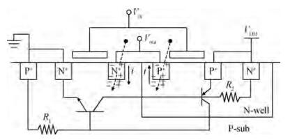
The cross-sectional view of an inverter with its parasitic latch-up structure shown. High energy particle striking the drains of the inverter creates a transient in the logic path
SEMICONDUCTOR INTEGRATED CIRCUITS
Gang Chen1, 2, Bo Gao1, 2 and Min Gong1, 2,
Corresponding author: Gong Min, Email:mgong@scu.edu.cn
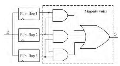
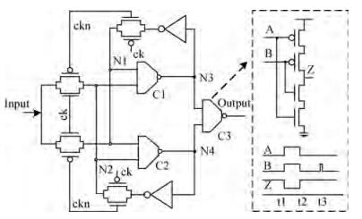
Abstract: A radiation-hardened flip-flop is proposed to mitigate the single event upset (SEU) effect. Immunity was achieved through the use of C-elements and redundant storage elements. It takes advantage of the property of a C-element in which it enters a high impedance mode when its inputs are of different logic values. Redundant storage nodes are then used to drive the C-elements so that a single upset pulse in any storage will be prevented from altering the state of the output of the flip-flop. The flip-flop was implemented using 48 transistors and occupied an area of 30.78 μm2, using 65 nm CMOS process. It consumed 22.6% fewer transistors as compared to the traditional SEU resilient TMR flip-flop.
Keywords: single event effect, radiation hardening by design, triple modular redundancy flip-flop, C-element
| [1] |
Nicolaidis M. Design for soft error mitigation. IEEE Trans Device Mater Reliab, 2005, 5(3):405 doi: 10.1109/TDMR.2005.855790
|
| [2] |
Dodd P E, Shaneyfelt M R, Schwank J R, et al. Current and future challenges in radiation effects on CMOS electronics. IEEE Trans Nucl Sci, 2010, 57(4):1747 doi: 10.1109/TNS.2010.2042613
|
| [3] |
Mavis D, Alexander D. Employing radiation hardness by design techniques with commercial integrated circuit processes. AIAA/IEEE 16th Digital Avionics Systems Conference, 1997, 1:2.1 http://ieeexplore.ieee.org/document/635027/authors
|
| [4] |
She X, Samudrala P. Selective triple modular redundancy for single event upset (SEU) mitigation. NASA/ESA Conference on Adaptive Hardware and Systems, 2009:344 http://dl.acm.org/citation.cfm?id=1673216
|
| [5] |
She X, McElvain K S. Time multiplexed triple modular redundancy for single event upset mitigation. IEEE Trans Nucl Sci, 2009, 56(4):2443 doi: 10.1109/TNS.2009.2021656
|
| [6] |
Wang X. Partitioning triple modular redundancy for single event upset mitigation in FPGA. International Conference on E-Product E-Service and E-Entertainment (ICEEE), 2010, 1:7 http://ieeexplore.ieee.org/document/5660842/authors
|
| [7] |
Oliveira R, Jagirdar A, Chakraborty T J. A TMR scheme for SEU mitigation in scan flip-flops. Proc 8th Int Symp Quality Electronic Design, 2007:905 http://ieeexplore.ieee.org/document/4149148/
|
| [8] |
Golshan S, Bozorgzadeh E. SEU-aware resource binding for modular redundancy based designs on FPGAs. Design, Automation & Test in Europe Conference & Exhibition, 2009:1124 http://dl.acm.org/citation.cfm?id=1874892&dl=ACM&coll=DL&CFID=988920426&CFTOKEN=93551803
|
| [9] |
Rennie D J, Sachdev M. Novel soft error robust flip-flops in 65 nm CMOS. IEEE Trans Nucl Sci, 2011, 58(5):2470 doi: 10.1109/TNS.2011.2162745
|
| [10] |
Mitra S, Ming Z, Waqas S, et al. Combinational logic soft error correction. Proc International Test Conference, 2006:1
|
| [11] |
Fazeli M, Patooghy A, Miremadi S G, et al. Feed-back redundancy:a power efficient SEU-tolerant latch design for deep sub-micron technologies. Proc 37th Annu IEEE/IFIP Int Conf Depend Syst Netw, 2007:276
|
| [12] |
Huang Zhengfeng, Liang Huaguo. A novel radiation hardened by design latch. Journal of Semiconductors, 2009, 30(3):035007 doi: 10.1088/1674-4926/30/3/035007
|
| [13] |
Wu Lihua, Han Xiaowei, Zhao Yan, et al. Design and implementation of a programming circuit in radiation-hardened FPGA. Journal of Semiconductors, 2011, 32(8):085012 doi: 10.1088/1674-4926/32/8/085012
|
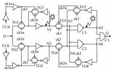
Table 1. Implementation results of the proposed flip-flop

|
| [1] |
Nicolaidis M. Design for soft error mitigation. IEEE Trans Device Mater Reliab, 2005, 5(3):405 doi: 10.1109/TDMR.2005.855790
|
| [2] |
Dodd P E, Shaneyfelt M R, Schwank J R, et al. Current and future challenges in radiation effects on CMOS electronics. IEEE Trans Nucl Sci, 2010, 57(4):1747 doi: 10.1109/TNS.2010.2042613
|
| [3] |
Mavis D, Alexander D. Employing radiation hardness by design techniques with commercial integrated circuit processes. AIAA/IEEE 16th Digital Avionics Systems Conference, 1997, 1:2.1 http://ieeexplore.ieee.org/document/635027/authors
|
| [4] |
She X, Samudrala P. Selective triple modular redundancy for single event upset (SEU) mitigation. NASA/ESA Conference on Adaptive Hardware and Systems, 2009:344 http://dl.acm.org/citation.cfm?id=1673216
|
| [5] |
She X, McElvain K S. Time multiplexed triple modular redundancy for single event upset mitigation. IEEE Trans Nucl Sci, 2009, 56(4):2443 doi: 10.1109/TNS.2009.2021656
|
| [6] |
Wang X. Partitioning triple modular redundancy for single event upset mitigation in FPGA. International Conference on E-Product E-Service and E-Entertainment (ICEEE), 2010, 1:7 http://ieeexplore.ieee.org/document/5660842/authors
|
| [7] |
Oliveira R, Jagirdar A, Chakraborty T J. A TMR scheme for SEU mitigation in scan flip-flops. Proc 8th Int Symp Quality Electronic Design, 2007:905 http://ieeexplore.ieee.org/document/4149148/
|
| [8] |
Golshan S, Bozorgzadeh E. SEU-aware resource binding for modular redundancy based designs on FPGAs. Design, Automation & Test in Europe Conference & Exhibition, 2009:1124 http://dl.acm.org/citation.cfm?id=1874892&dl=ACM&coll=DL&CFID=988920426&CFTOKEN=93551803
|
| [9] |
Rennie D J, Sachdev M. Novel soft error robust flip-flops in 65 nm CMOS. IEEE Trans Nucl Sci, 2011, 58(5):2470 doi: 10.1109/TNS.2011.2162745
|
| [10] |
Mitra S, Ming Z, Waqas S, et al. Combinational logic soft error correction. Proc International Test Conference, 2006:1
|
| [11] |
Fazeli M, Patooghy A, Miremadi S G, et al. Feed-back redundancy:a power efficient SEU-tolerant latch design for deep sub-micron technologies. Proc 37th Annu IEEE/IFIP Int Conf Depend Syst Netw, 2007:276
|
| [12] |
Huang Zhengfeng, Liang Huaguo. A novel radiation hardened by design latch. Journal of Semiconductors, 2009, 30(3):035007 doi: 10.1088/1674-4926/30/3/035007
|
| [13] |
Wu Lihua, Han Xiaowei, Zhao Yan, et al. Design and implementation of a programming circuit in radiation-hardened FPGA. Journal of Semiconductors, 2011, 32(8):085012 doi: 10.1088/1674-4926/32/8/085012
|


Article views: 3459 Times PDF downloads: 31 Times Cited by: 0 Times
Received: 16 January 2013 Revised: 25 March 2013 Online: Published: 01 September 2013
| Citation: |
Gang Chen, Bo Gao, Min Gong. A dual redundancy radiation-hardened flip-flop based on a C-element in a 65 nm process[J]. Journal of Semiconductors, 2013, 34(9): 095012. doi: 10.1088/1674-4926/34/9/095012
****
G Chen, B Gao, M Gong. A dual redundancy radiation-hardened flip-flop based on a C-element in a 65 nm process[J]. J. Semicond., 2013, 34(9): 095012. doi: 10.1088/1674-4926/34/9/095012.

|
| [1] |
Nicolaidis M. Design for soft error mitigation. IEEE Trans Device Mater Reliab, 2005, 5(3):405 doi: 10.1109/TDMR.2005.855790
|
| [2] |
Dodd P E, Shaneyfelt M R, Schwank J R, et al. Current and future challenges in radiation effects on CMOS electronics. IEEE Trans Nucl Sci, 2010, 57(4):1747 doi: 10.1109/TNS.2010.2042613
|
| [3] |
Mavis D, Alexander D. Employing radiation hardness by design techniques with commercial integrated circuit processes. AIAA/IEEE 16th Digital Avionics Systems Conference, 1997, 1:2.1 http://ieeexplore.ieee.org/document/635027/authors
|
| [4] |
She X, Samudrala P. Selective triple modular redundancy for single event upset (SEU) mitigation. NASA/ESA Conference on Adaptive Hardware and Systems, 2009:344 http://dl.acm.org/citation.cfm?id=1673216
|
| [5] |
She X, McElvain K S. Time multiplexed triple modular redundancy for single event upset mitigation. IEEE Trans Nucl Sci, 2009, 56(4):2443 doi: 10.1109/TNS.2009.2021656
|
| [6] |
Wang X. Partitioning triple modular redundancy for single event upset mitigation in FPGA. International Conference on E-Product E-Service and E-Entertainment (ICEEE), 2010, 1:7 http://ieeexplore.ieee.org/document/5660842/authors
|
| [7] |
Oliveira R, Jagirdar A, Chakraborty T J. A TMR scheme for SEU mitigation in scan flip-flops. Proc 8th Int Symp Quality Electronic Design, 2007:905 http://ieeexplore.ieee.org/document/4149148/
|
| [8] |
Golshan S, Bozorgzadeh E. SEU-aware resource binding for modular redundancy based designs on FPGAs. Design, Automation & Test in Europe Conference & Exhibition, 2009:1124 http://dl.acm.org/citation.cfm?id=1874892&dl=ACM&coll=DL&CFID=988920426&CFTOKEN=93551803
|
| [9] |
Rennie D J, Sachdev M. Novel soft error robust flip-flops in 65 nm CMOS. IEEE Trans Nucl Sci, 2011, 58(5):2470 doi: 10.1109/TNS.2011.2162745
|
| [10] |
Mitra S, Ming Z, Waqas S, et al. Combinational logic soft error correction. Proc International Test Conference, 2006:1
|
| [11] |
Fazeli M, Patooghy A, Miremadi S G, et al. Feed-back redundancy:a power efficient SEU-tolerant latch design for deep sub-micron technologies. Proc 37th Annu IEEE/IFIP Int Conf Depend Syst Netw, 2007:276
|
| [12] |
Huang Zhengfeng, Liang Huaguo. A novel radiation hardened by design latch. Journal of Semiconductors, 2009, 30(3):035007 doi: 10.1088/1674-4926/30/3/035007
|
| [13] |
Wu Lihua, Han Xiaowei, Zhao Yan, et al. Design and implementation of a programming circuit in radiation-hardened FPGA. Journal of Semiconductors, 2011, 32(8):085012 doi: 10.1088/1674-4926/32/8/085012
|

 WeChat ID
Journal of Semiconductors © 2017 All Rights Reserved 京ICP备05085259号-2

 DownLoad: