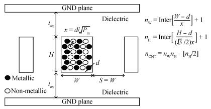
Fig. 1.
Cross-section view of the geometry of the SWCNT bundle interconnects
SEMICONDUCTOR INTEGRATED CIRCUITS
Libo Qian, Zhangming Zhu, Ruixue Ding and Yintang Yang
Corresponding author: Zhu Zhangming, Email:zhangmingzhu@xidian.edu.cn
Abstract: Metallic carbon nanotubes (CNTs) have been proposed as a promising alternative to Cu interconnects in future integrated circuits (ICs) for their remarkable conductive, mechanical and thermal properties. Compact equivalent circuit models for single-walled carbon nanotube (SWCNT) bundles are described, and the performance of SWCNT bundle interconnects is evaluated and compared with traditional Cu interconnects at different interconnect levels for through-silicon-via-based three dimensional (3D) ICs. It is shown that at a local level, CNT interconnects exhibit lower signal delay and smaller optimal wire size. At intermediate and global levels, the delay improvement becomes more significant with technology scaling and increasing wire lengths. For 1 mm intermediate and 10 mm global level interconnects, the delay of SWCNT bundles is only 49.49% and 52.82% that of the Cu wires, respectively.
Keywords: three-dimensional integrated circuits (3D ICs), carbon nanotube (CNT), signal delay, repeater insertion
| [1] |
Pavlidis V F, Friedman E G. Three-dimensional integrated circuit design. San Mateo:Morgan Kaufmann, 2009
|
| [2] |
Xie Y, Cong J, Sapatnekar S. Three-dimensional integrated circuit design. New York:Springer, 2010
|
| [3] |
Steinhogl W, Schindler G, Engelhardt M. Size dependent resistivity of metallic wires in the mesoscopic range. Phys Rev B:Condens Matter 2002, 66(7):075414 doi: 10.1103/PhysRevB.66.075414
|
| [4] |
Ryu C, Kwon K W, Loke A L S, et al. Microstructure and reliability of copper interconnect. IEEE Trans Electron Devices, 1999, 46(6):1113 doi: 10.1109/16.766872
|
| [5] |
McEuen P L, Fuhrer M S, Park H K. Single-walled carbon nanotube electronics. IEEE Trans Nanotechnology, 2007, 79(8):1172
|
| [6] |
Zhang Z H, Peng J C, Chen X H, et al. Current properties in doped single walled carbon nanotubes. Journal of Semiconductors, 2002, 23(5):499
|
| [7] |
Zhan L F, Hu H F. Effect of topological defects on carbon nanotube. Journal of Semiconductors, 2005, 26(10):1959
|
| [8] |
Li H, Yin W Y, Banerjee K, et al. Circuit modeling and performance analysis of multi-walled carbon nanotube interconnects. IEEE Electron Devices, 2008, 55(6):1328 doi: 10.1109/TED.2008.922855
|
| [9] |
Wei B Q, Vajtai R, Ajayan P M. Reliability and current carrying capacity of carbon nanotubes. Appl Phys Lett, 2010, 96(4):1161
|
| [10] |
Banerjee K, Srivastava N. Are carbon nanotubes the future of VLSI interconnect. Proc IEEE/ACM Design Autom Conf, 2006:809
|
| [11] |
Koo K H, Cho H, Kapur P, et al. Performance comparison between carbon nanotubes, optical, and Cu for future high performance on chip interconnects application. IEEE Trans Electron Devices, 2007, 54(12):3206 doi: 10.1109/TED.2007.909045
|
| [12] |
Naeemi A, Sarvari R, Meindl J. Performance comparison between carbon nanotube and copper interconnect for gigascale intergration (GSI). IEEE Trans Electron Device Lett, 2005, 26(2):84 doi: 10.1109/LED.2004.841440
|
| [13] |
Fang Z. Transmission line model of carbon nanotubes:through the Boltzmann transport equation. Journal of Semiconductors, 2011, 32(6):062002 doi: 10.1088/1674-4926/32/6/062002
|
| [14] |
Naeemi A, Meindl J. Design and performance modeling for single walled carbon nanotubes as local, semiglobal and global interconnects in giga-scale integrated circuits. IEEE Trans Electron Devices, 2007, 54(1):26 doi: 10.1109/TED.2006.887210
|
| [15] |
Ceyhan A, Naeemi A. Cu interconnects limitations and opportunities for SWNT interconnect at the end of the roadmap. IEEE Trans Electron Device, 2013, 60(1):374 doi: 10.1109/TED.2012.2224663
|
| [16] |
Srivastava N, Banerjee K. Performance analysis of carbon nanotube interconnects for VLSI applications. Proc IEEE/ACM Int Conf ICCAD, 2005:383
|
| [17] |
Pasricha S, Dutt N, Kurdahi F J. Exploring carbon nanotube bundle global interconnects for chip multiprocessor applications. Int Conf VLSI Design, 2009:499
|
| [18] |
Park J Y, Rosenbelt S, Yaish Y, et al. Electron-phonon scattering in metallic single wall carbon nanotubes. Nano Lett, 2004, 4:517 doi: 10.1021/nl035258c
|
| [19] |
Nieuwoudt A, Massoud Y. Evaluation the impact of resistance in carbon nanotube bundle for VLSI interconnects using diameter-dependent modeling techniques. IEEE Trans Electron Devices, 2006, 53(10):2460 doi: 10.1109/TED.2006.882035
|
| [20] |
Naeemi A, Meindl J. Performance modeling for single-and multiwall carbon nanotubes as signal and power interconnects in gigascale systems. IEEE Electron Device, 2008, 55(10):2574 doi: 10.1109/TED.2008.2003028
|
| [21] |
Burke P J. Luttinger liquid theory as a model of the gigahertz electrical properties of carbon nanotubes. IEEE Trans Nanotechnology, 2001, 1(3):129
|
| [22] |
HSPICE Manuals, Synopsis Inc. , Mountain View, CA, 2003
|
| [23] |
International Technology Roadmap for Semiconductors, 2009. [Online]. Available: http://www.itrs.net/
|
| [24] |
Predictive Technology Model (PTM). [Online]. Available: http://ptm.asu.edu/
|
| [25] |
Kuznetsov A R, Hewaparakrama K, Kim S M, et al. Preferential growth of single walled carbon nanotubes with metallic conductivity. Science 2009, 326(5949):116 doi: 10.1126/science.1177599
|
| [26] |
Katti G, Stucchi M, Meyer K D, et al. Electrical modeling and characterization of through silicon via for three dimensional ICs. IEEE Trans Electron Devices, 2010, 57(1):256 doi: 10.1109/TED.2009.2034508
|
| [27] |
Savidis I, Friedman E G. Closed form expression of 3D via resistance, inductance, and capacitance. IEEE Trans Electron Devices, 2009, 56(9):1873 doi: 10.1109/TED.2009.2026200
|
| [28] |
Xu C, Li H, Kaustav B. Compact AC modeling and performance analysis of through silicon vias in 3D ICs. IEEE Trans Electron Devices, 2010, 57(12):3405 doi: 10.1109/TED.2010.2076382
|
| [29] |
Xu H, Pavlidis V F, Micheli G D. Repeater insertion for two terminal nets in three dimensional integrated circuits. Proc 4th NanoNet Conference, 2009:141
|
| [30] |
Ismail Y I, Friedman E G. Effect of inductance on the propagation delay and repeater insertion in VLSI circuits. IEEE Trans VLSI Syst, 2000, 8(2):195 doi: 10.1109/92.831439
|
| [31] |
Liang F, Wang G F, Ding W. Estimation of time delay and repeater insertion in multiwall carbon nanotube interconnects. IEEE Trans Electron Devices, 2011, 58(8):2712 doi: 10.1109/TED.2011.2154334
|
| [32] |
Qian L, Zhu Z. Analytical heat transfer model for three dimensional integrated circuits incorporating through silicon via effect. IET Mirco & Nano Lett, 2012, 7(9):994
|
| [33] |
Wang T, Jeppson K, Yem L L, et al. Carbon nanotube through silicon via interconnects for three dimensional integration. Small, 2011, 7(16):2313 doi: 10.1002/smll.v7.16
|
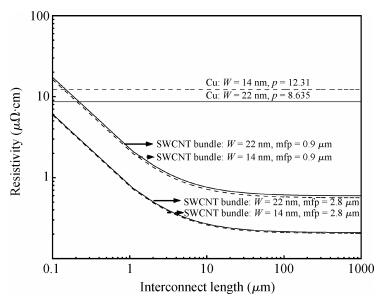
Table 1. The ITRS 2009-based simulation parameters

|
Table 2. Comparison of the optimal number and size of repeaters in the intermediate and global interconnects for different technology nodes

|
| [1] |
Pavlidis V F, Friedman E G. Three-dimensional integrated circuit design. San Mateo:Morgan Kaufmann, 2009
|
| [2] |
Xie Y, Cong J, Sapatnekar S. Three-dimensional integrated circuit design. New York:Springer, 2010
|
| [3] |
Steinhogl W, Schindler G, Engelhardt M. Size dependent resistivity of metallic wires in the mesoscopic range. Phys Rev B:Condens Matter 2002, 66(7):075414 doi: 10.1103/PhysRevB.66.075414
|
| [4] |
Ryu C, Kwon K W, Loke A L S, et al. Microstructure and reliability of copper interconnect. IEEE Trans Electron Devices, 1999, 46(6):1113 doi: 10.1109/16.766872
|
| [5] |
McEuen P L, Fuhrer M S, Park H K. Single-walled carbon nanotube electronics. IEEE Trans Nanotechnology, 2007, 79(8):1172
|
| [6] |
Zhang Z H, Peng J C, Chen X H, et al. Current properties in doped single walled carbon nanotubes. Journal of Semiconductors, 2002, 23(5):499
|
| [7] |
Zhan L F, Hu H F. Effect of topological defects on carbon nanotube. Journal of Semiconductors, 2005, 26(10):1959
|
| [8] |
Li H, Yin W Y, Banerjee K, et al. Circuit modeling and performance analysis of multi-walled carbon nanotube interconnects. IEEE Electron Devices, 2008, 55(6):1328 doi: 10.1109/TED.2008.922855
|
| [9] |
Wei B Q, Vajtai R, Ajayan P M. Reliability and current carrying capacity of carbon nanotubes. Appl Phys Lett, 2010, 96(4):1161
|
| [10] |
Banerjee K, Srivastava N. Are carbon nanotubes the future of VLSI interconnect. Proc IEEE/ACM Design Autom Conf, 2006:809
|
| [11] |
Koo K H, Cho H, Kapur P, et al. Performance comparison between carbon nanotubes, optical, and Cu for future high performance on chip interconnects application. IEEE Trans Electron Devices, 2007, 54(12):3206 doi: 10.1109/TED.2007.909045
|
| [12] |
Naeemi A, Sarvari R, Meindl J. Performance comparison between carbon nanotube and copper interconnect for gigascale intergration (GSI). IEEE Trans Electron Device Lett, 2005, 26(2):84 doi: 10.1109/LED.2004.841440
|
| [13] |
Fang Z. Transmission line model of carbon nanotubes:through the Boltzmann transport equation. Journal of Semiconductors, 2011, 32(6):062002 doi: 10.1088/1674-4926/32/6/062002
|
| [14] |
Naeemi A, Meindl J. Design and performance modeling for single walled carbon nanotubes as local, semiglobal and global interconnects in giga-scale integrated circuits. IEEE Trans Electron Devices, 2007, 54(1):26 doi: 10.1109/TED.2006.887210
|
| [15] |
Ceyhan A, Naeemi A. Cu interconnects limitations and opportunities for SWNT interconnect at the end of the roadmap. IEEE Trans Electron Device, 2013, 60(1):374 doi: 10.1109/TED.2012.2224663
|
| [16] |
Srivastava N, Banerjee K. Performance analysis of carbon nanotube interconnects for VLSI applications. Proc IEEE/ACM Int Conf ICCAD, 2005:383
|
| [17] |
Pasricha S, Dutt N, Kurdahi F J. Exploring carbon nanotube bundle global interconnects for chip multiprocessor applications. Int Conf VLSI Design, 2009:499
|
| [18] |
Park J Y, Rosenbelt S, Yaish Y, et al. Electron-phonon scattering in metallic single wall carbon nanotubes. Nano Lett, 2004, 4:517 doi: 10.1021/nl035258c
|
| [19] |
Nieuwoudt A, Massoud Y. Evaluation the impact of resistance in carbon nanotube bundle for VLSI interconnects using diameter-dependent modeling techniques. IEEE Trans Electron Devices, 2006, 53(10):2460 doi: 10.1109/TED.2006.882035
|
| [20] |
Naeemi A, Meindl J. Performance modeling for single-and multiwall carbon nanotubes as signal and power interconnects in gigascale systems. IEEE Electron Device, 2008, 55(10):2574 doi: 10.1109/TED.2008.2003028
|
| [21] |
Burke P J. Luttinger liquid theory as a model of the gigahertz electrical properties of carbon nanotubes. IEEE Trans Nanotechnology, 2001, 1(3):129
|
| [22] |
HSPICE Manuals, Synopsis Inc. , Mountain View, CA, 2003
|
| [23] |
International Technology Roadmap for Semiconductors, 2009. [Online]. Available: http://www.itrs.net/
|
| [24] |
Predictive Technology Model (PTM). [Online]. Available: http://ptm.asu.edu/
|
| [25] |
Kuznetsov A R, Hewaparakrama K, Kim S M, et al. Preferential growth of single walled carbon nanotubes with metallic conductivity. Science 2009, 326(5949):116 doi: 10.1126/science.1177599
|
| [26] |
Katti G, Stucchi M, Meyer K D, et al. Electrical modeling and characterization of through silicon via for three dimensional ICs. IEEE Trans Electron Devices, 2010, 57(1):256 doi: 10.1109/TED.2009.2034508
|
| [27] |
Savidis I, Friedman E G. Closed form expression of 3D via resistance, inductance, and capacitance. IEEE Trans Electron Devices, 2009, 56(9):1873 doi: 10.1109/TED.2009.2026200
|
| [28] |
Xu C, Li H, Kaustav B. Compact AC modeling and performance analysis of through silicon vias in 3D ICs. IEEE Trans Electron Devices, 2010, 57(12):3405 doi: 10.1109/TED.2010.2076382
|
| [29] |
Xu H, Pavlidis V F, Micheli G D. Repeater insertion for two terminal nets in three dimensional integrated circuits. Proc 4th NanoNet Conference, 2009:141
|
| [30] |
Ismail Y I, Friedman E G. Effect of inductance on the propagation delay and repeater insertion in VLSI circuits. IEEE Trans VLSI Syst, 2000, 8(2):195 doi: 10.1109/92.831439
|
| [31] |
Liang F, Wang G F, Ding W. Estimation of time delay and repeater insertion in multiwall carbon nanotube interconnects. IEEE Trans Electron Devices, 2011, 58(8):2712 doi: 10.1109/TED.2011.2154334
|
| [32] |
Qian L, Zhu Z. Analytical heat transfer model for three dimensional integrated circuits incorporating through silicon via effect. IET Mirco & Nano Lett, 2012, 7(9):994
|
| [33] |
Wang T, Jeppson K, Yem L L, et al. Carbon nanotube through silicon via interconnects for three dimensional integration. Small, 2011, 7(16):2313 doi: 10.1002/smll.v7.16
|


Article views: 3344 Times PDF downloads: 20 Times Cited by: 0 Times
Received: 28 February 2013 Revised: 07 April 2013 Online: Published: 01 September 2013
| Citation: |
Libo Qian, Zhangming Zhu, Ruixue Ding, Yintang Yang. Circuit modeling and performance analysis of SWCNT bundle 3D interconnects[J]. Journal of Semiconductors, 2013, 34(9): 095014. doi: 10.1088/1674-4926/34/9/095014
****
L B Qian, Z M Zhu, R X Ding, Y T Yang. Circuit modeling and performance analysis of SWCNT bundle 3D interconnects[J]. J. Semicond., 2013, 34(9): 095014. doi: 10.1088/1674-4926/34/9/095014.

|
| [1] |
Pavlidis V F, Friedman E G. Three-dimensional integrated circuit design. San Mateo:Morgan Kaufmann, 2009
|
| [2] |
Xie Y, Cong J, Sapatnekar S. Three-dimensional integrated circuit design. New York:Springer, 2010
|
| [3] |
Steinhogl W, Schindler G, Engelhardt M. Size dependent resistivity of metallic wires in the mesoscopic range. Phys Rev B:Condens Matter 2002, 66(7):075414 doi: 10.1103/PhysRevB.66.075414
|
| [4] |
Ryu C, Kwon K W, Loke A L S, et al. Microstructure and reliability of copper interconnect. IEEE Trans Electron Devices, 1999, 46(6):1113 doi: 10.1109/16.766872
|
| [5] |
McEuen P L, Fuhrer M S, Park H K. Single-walled carbon nanotube electronics. IEEE Trans Nanotechnology, 2007, 79(8):1172
|
| [6] |
Zhang Z H, Peng J C, Chen X H, et al. Current properties in doped single walled carbon nanotubes. Journal of Semiconductors, 2002, 23(5):499
|
| [7] |
Zhan L F, Hu H F. Effect of topological defects on carbon nanotube. Journal of Semiconductors, 2005, 26(10):1959
|
| [8] |
Li H, Yin W Y, Banerjee K, et al. Circuit modeling and performance analysis of multi-walled carbon nanotube interconnects. IEEE Electron Devices, 2008, 55(6):1328 doi: 10.1109/TED.2008.922855
|
| [9] |
Wei B Q, Vajtai R, Ajayan P M. Reliability and current carrying capacity of carbon nanotubes. Appl Phys Lett, 2010, 96(4):1161
|
| [10] |
Banerjee K, Srivastava N. Are carbon nanotubes the future of VLSI interconnect. Proc IEEE/ACM Design Autom Conf, 2006:809
|
| [11] |
Koo K H, Cho H, Kapur P, et al. Performance comparison between carbon nanotubes, optical, and Cu for future high performance on chip interconnects application. IEEE Trans Electron Devices, 2007, 54(12):3206 doi: 10.1109/TED.2007.909045
|
| [12] |
Naeemi A, Sarvari R, Meindl J. Performance comparison between carbon nanotube and copper interconnect for gigascale intergration (GSI). IEEE Trans Electron Device Lett, 2005, 26(2):84 doi: 10.1109/LED.2004.841440
|
| [13] |
Fang Z. Transmission line model of carbon nanotubes:through the Boltzmann transport equation. Journal of Semiconductors, 2011, 32(6):062002 doi: 10.1088/1674-4926/32/6/062002
|
| [14] |
Naeemi A, Meindl J. Design and performance modeling for single walled carbon nanotubes as local, semiglobal and global interconnects in giga-scale integrated circuits. IEEE Trans Electron Devices, 2007, 54(1):26 doi: 10.1109/TED.2006.887210
|
| [15] |
Ceyhan A, Naeemi A. Cu interconnects limitations and opportunities for SWNT interconnect at the end of the roadmap. IEEE Trans Electron Device, 2013, 60(1):374 doi: 10.1109/TED.2012.2224663
|
| [16] |
Srivastava N, Banerjee K. Performance analysis of carbon nanotube interconnects for VLSI applications. Proc IEEE/ACM Int Conf ICCAD, 2005:383
|
| [17] |
Pasricha S, Dutt N, Kurdahi F J. Exploring carbon nanotube bundle global interconnects for chip multiprocessor applications. Int Conf VLSI Design, 2009:499
|
| [18] |
Park J Y, Rosenbelt S, Yaish Y, et al. Electron-phonon scattering in metallic single wall carbon nanotubes. Nano Lett, 2004, 4:517 doi: 10.1021/nl035258c
|
| [19] |
Nieuwoudt A, Massoud Y. Evaluation the impact of resistance in carbon nanotube bundle for VLSI interconnects using diameter-dependent modeling techniques. IEEE Trans Electron Devices, 2006, 53(10):2460 doi: 10.1109/TED.2006.882035
|
| [20] |
Naeemi A, Meindl J. Performance modeling for single-and multiwall carbon nanotubes as signal and power interconnects in gigascale systems. IEEE Electron Device, 2008, 55(10):2574 doi: 10.1109/TED.2008.2003028
|
| [21] |
Burke P J. Luttinger liquid theory as a model of the gigahertz electrical properties of carbon nanotubes. IEEE Trans Nanotechnology, 2001, 1(3):129
|
| [22] |
HSPICE Manuals, Synopsis Inc. , Mountain View, CA, 2003
|
| [23] |
International Technology Roadmap for Semiconductors, 2009. [Online]. Available: http://www.itrs.net/
|
| [24] |
Predictive Technology Model (PTM). [Online]. Available: http://ptm.asu.edu/
|
| [25] |
Kuznetsov A R, Hewaparakrama K, Kim S M, et al. Preferential growth of single walled carbon nanotubes with metallic conductivity. Science 2009, 326(5949):116 doi: 10.1126/science.1177599
|
| [26] |
Katti G, Stucchi M, Meyer K D, et al. Electrical modeling and characterization of through silicon via for three dimensional ICs. IEEE Trans Electron Devices, 2010, 57(1):256 doi: 10.1109/TED.2009.2034508
|
| [27] |
Savidis I, Friedman E G. Closed form expression of 3D via resistance, inductance, and capacitance. IEEE Trans Electron Devices, 2009, 56(9):1873 doi: 10.1109/TED.2009.2026200
|
| [28] |
Xu C, Li H, Kaustav B. Compact AC modeling and performance analysis of through silicon vias in 3D ICs. IEEE Trans Electron Devices, 2010, 57(12):3405 doi: 10.1109/TED.2010.2076382
|
| [29] |
Xu H, Pavlidis V F, Micheli G D. Repeater insertion for two terminal nets in three dimensional integrated circuits. Proc 4th NanoNet Conference, 2009:141
|
| [30] |
Ismail Y I, Friedman E G. Effect of inductance on the propagation delay and repeater insertion in VLSI circuits. IEEE Trans VLSI Syst, 2000, 8(2):195 doi: 10.1109/92.831439
|
| [31] |
Liang F, Wang G F, Ding W. Estimation of time delay and repeater insertion in multiwall carbon nanotube interconnects. IEEE Trans Electron Devices, 2011, 58(8):2712 doi: 10.1109/TED.2011.2154334
|
| [32] |
Qian L, Zhu Z. Analytical heat transfer model for three dimensional integrated circuits incorporating through silicon via effect. IET Mirco & Nano Lett, 2012, 7(9):994
|
| [33] |
Wang T, Jeppson K, Yem L L, et al. Carbon nanotube through silicon via interconnects for three dimensional integration. Small, 2011, 7(16):2313 doi: 10.1002/smll.v7.16
|

 WeChat ID
Journal of Semiconductors © 2017 All Rights Reserved 京ICP备05085259号-2

 DownLoad: