


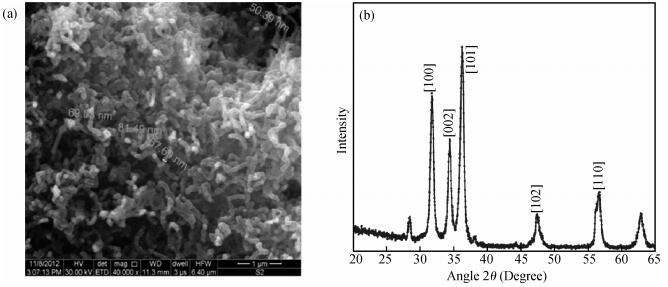
Fig. 1.
(a) SEM image and (b) XRD spectra of the as-prepared ZnO nanowire thin film on a SiNW array substrate.
SEMICONDUCTOR DEVICES
Purnima Hazra and S. Jit
Corresponding author: Purnima Hazra, Email: phazra.rs.ece@itbhu.ac.in
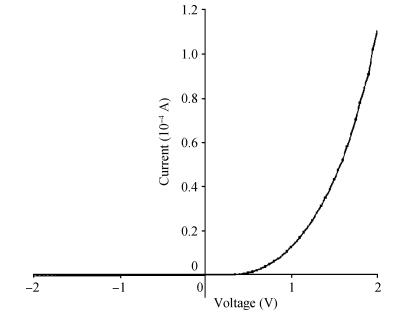
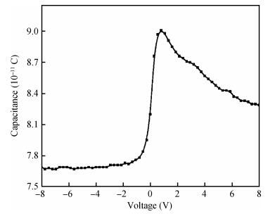
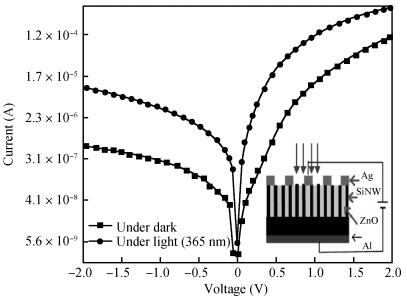
Abstract: This paper represents the electrical and optical characteristics of a SiNW/ZnO heterojunction diode and subsequent studies on the photodetection properties of the diode in the ultraviolet (UV) wavelength region. In this work, silicon nanowire arrays were prepared on p-type (100)-oriented Si substrate by an electroless metal deposition and etching method with the help of ultrasonication. After that, catalyst-free deposition of zinc oxide (ZnO) nanowires on a silicon nanowire (SiNW) array substrate was done by utilizing a simple and cost-effective thermal evaporation technique without using a buffer layer. The SEM and XRD techniques are used to show the quality of the as-grown ZnO nanowire film. The junction properties of the diode are evaluated by measuring current-voltage and capacitance-voltage characteristics. The diode has a well-defined rectifying behavior with a rectification ratio of 190 at ±2 V, turn-on voltage of 0.5 V, and barrier height is 0.727 eV at room temperature under dark conditions. The photodetection parameters of the diode are investigated in the bias voltage range of ±2 V. The diode shows responsivity of 0.8 A/W at a bias voltage of 2 V under UV illumination (wavelength=365 nm). The characteristics of the device indicate that it can be used for UV detection applications in nano-optoelectronic and photonic devices.
Keywords: silicon nanowire, ZnO nanowire, heterojunction diode, interface, barrier height, photo responsivity
| [1] |
Ali G M, Singh S, Chakrabarti P. Ultraviolet ZnO photodetectors with high gain. J Electron Sci Technol, 2010, 8(1):55
|
| [2] |
Periasamy C, Chakrabarti P. Electrical and optical characterization of ZnO based nano and large area Schottky contacts. Curr Appl Phys, 2011, 11(4):959 doi: 10.1016/j.cap.2010.10.007
|
| [3] |
Chirakkara S, Krupanidhi S B. Study of n-ZnO/p-Si (100) thin film heterojunctions by pulsed laser deposition without buffer layer. Thin Solid Films, 2012, 520(18):5894 doi: 10.1016/j.tsf.2012.05.003
|
| [4] |
Vaezi M R, Sadrnezhaad S K. Effects of substrate material and annealing temperature on morphology of zinc oxide films. Mater Sci Technol, 2006, 22(3):308 doi: 10.1179/174328406X78361
|
| [5] |
Ding J N, Liu Y B, Tan C B, et al. Investigations into the impact of various substrates and ZnO ultra thin seed layers prepared by atomic layer deposition on growth of ZnO nanowire array. Nanoscale Res Lett, 2012, 7(1):368 doi: 10.1186/1556-276X-7-368
|
| [6] |
Minami T, Miyata T, Ihara K, et al. Effect of ZnO film deposition methods on the photovoltaic properties of ZnO-Cu2O heterojunction devices. Thin Solid Films, 2006, 494(1/2):47
|
| [7] |
Polsongkram D, Chamninok P, Pukird S, et al. Effect of synthesis conditions on the growth of ZnO nanorods via hydrothermal method. Physica B, 2008, 403(19/20):3713
|
| [8] |
Um H D, Moiz S A, Park K T, et al. Highly selective spectral response with enhanced responsivity of n-ZnO/p-Si radial heterojunction nanowire photodiode. Appl Phys Lett, 2011, 98(3):033102 doi: 10.1063/1.3543845
|
| [9] |
Kale V S, Prabhakar R R, Pramana S S, et al. Enhanced electron field emission properties of high aspect ratio silicon nanowire-zinc oxide core-shell arrays. Phys Chem Chem Phys, 2012, 14(13):4614 doi: 10.1039/c2cp40238f
|
| [10] |
Kang H, Park J, Choi T, et al. n-ZnO:N/p-Si nanowire photodiode prepared by atomic layer deposition. Appl Phys Lett, 2012, 100(4):041117 doi: 10.1063/1.3679078
|
| [11] |
Sun L, He H, Liu C, et al. Controllable growth and optical properties of ZnO nanostructures on Si nanowire arrays. Cryst Engg Comm, 2011, 13(7):2439 doi: 10.1039/c0ce00844c
|
| [12] |
Sun K, Jing Y, Park N, et al. Solution synthesis of large-scale, high-sensitivity ZnO/Si hierarchical nanoheterostructure photodetectors. J Am Chem Soc, 2010, 132(44):15465 doi: 10.1021/ja1038424
|
| [13] |
Choi J H, Das S N, Moon K J, et al. Fabrication and characterization of p-Si nanowires/ZnO film heterojunction diode. Solid-State Electron, 2010, 54(12):1582 doi: 10.1016/j.sse.2010.07.015
|
| [14] |
Zhou H, Fang G, Yuan L, et al. Deep ultraviolet and near infrared photodiode based on n-ZnO/p-silicon nanowire heterojunction fabricated at low temperature. Appl Phys Lett, 2009, 94(1):013503 doi: 10.1063/1.3064161
|
| [15] |
Hu J, Chen Z, Sun Y, et al. ZnO-Si side-to-side biaxial nanowire heterostructures with improved luminescence. J Mater Chem, 2009, 19(38):7011 doi: 10.1039/b902201e
|
| [16] |
Kim K, Moona T, Lee M, et al. Light-emitting diodes composed of n-ZnO and p-Si nanowires constructed on plastic substrates by dielectrophoresis. Solid State Sci, 2011, 13(9):1735 doi: 10.1016/j.solidstatesciences.2011.06.028
|
| [17] |
Hazra P, Jit S. An In-house approach for fabrication of silicon nanowire arrays using electroless metal deposition and etching method. Int J Surf Sci Eng, 2013, 7(3):285 doi: 10.1504/IJSURFSE.2013.056439
|
| [18] |
Chen Y, Pu Y, Wang L, et al. Influence of nitrogen annealing on structural and photoluminescent properties of ZnO thin film grown on c-Al2O3 by atmospheric pressure MOCVD. Mat Sci Semicond Proc, 2005, 8(4):491 doi: 10.1016/j.mssp.2004.07.006
|
| [19] |
Yakuphanoglu F. The current-voltage characteristics of FSS/n-Si heterojunction diode under dark and illumination. Physica B, 2007, 388(1/2):226
|
| [20] |
Seo O, Kim H, Jo J. Anomalous capacitance change in low-temperature grown ZnO thin-film transistors. Eur Phys J Appl Phys, 2010, 52(1):10501 doi: 10.1051/epjap/2010129
|


Article views: 2981 Times PDF downloads: 25 Times Cited by: 0 Times
Received: 28 June 2013 Revised: 14 August 2013 Online: Published: 01 January 2014
| Citation: |
Purnima Hazra, S. Jit. A p-silicon nanowire/n-ZnO thin film heterojunction diode prepared by thermal evaporation[J]. Journal of Semiconductors, 2014, 35(1): 014001. doi: 10.1088/1674-4926/35/1/014001
****
P Hazra, S. Jit. A p-silicon nanowire/n-ZnO thin film heterojunction diode prepared by thermal evaporation[J]. J. Semicond., 2014, 35(1): 014001. doi: 10.1088/1674-4926/35/1/014001.

|
| [1] |
Ali G M, Singh S, Chakrabarti P. Ultraviolet ZnO photodetectors with high gain. J Electron Sci Technol, 2010, 8(1):55
|
| [2] |
Periasamy C, Chakrabarti P. Electrical and optical characterization of ZnO based nano and large area Schottky contacts. Curr Appl Phys, 2011, 11(4):959 doi: 10.1016/j.cap.2010.10.007
|
| [3] |
Chirakkara S, Krupanidhi S B. Study of n-ZnO/p-Si (100) thin film heterojunctions by pulsed laser deposition without buffer layer. Thin Solid Films, 2012, 520(18):5894 doi: 10.1016/j.tsf.2012.05.003
|
| [4] |
Vaezi M R, Sadrnezhaad S K. Effects of substrate material and annealing temperature on morphology of zinc oxide films. Mater Sci Technol, 2006, 22(3):308 doi: 10.1179/174328406X78361
|
| [5] |
Ding J N, Liu Y B, Tan C B, et al. Investigations into the impact of various substrates and ZnO ultra thin seed layers prepared by atomic layer deposition on growth of ZnO nanowire array. Nanoscale Res Lett, 2012, 7(1):368 doi: 10.1186/1556-276X-7-368
|
| [6] |
Minami T, Miyata T, Ihara K, et al. Effect of ZnO film deposition methods on the photovoltaic properties of ZnO-Cu2O heterojunction devices. Thin Solid Films, 2006, 494(1/2):47
|
| [7] |
Polsongkram D, Chamninok P, Pukird S, et al. Effect of synthesis conditions on the growth of ZnO nanorods via hydrothermal method. Physica B, 2008, 403(19/20):3713
|
| [8] |
Um H D, Moiz S A, Park K T, et al. Highly selective spectral response with enhanced responsivity of n-ZnO/p-Si radial heterojunction nanowire photodiode. Appl Phys Lett, 2011, 98(3):033102 doi: 10.1063/1.3543845
|
| [9] |
Kale V S, Prabhakar R R, Pramana S S, et al. Enhanced electron field emission properties of high aspect ratio silicon nanowire-zinc oxide core-shell arrays. Phys Chem Chem Phys, 2012, 14(13):4614 doi: 10.1039/c2cp40238f
|
| [10] |
Kang H, Park J, Choi T, et al. n-ZnO:N/p-Si nanowire photodiode prepared by atomic layer deposition. Appl Phys Lett, 2012, 100(4):041117 doi: 10.1063/1.3679078
|
| [11] |
Sun L, He H, Liu C, et al. Controllable growth and optical properties of ZnO nanostructures on Si nanowire arrays. Cryst Engg Comm, 2011, 13(7):2439 doi: 10.1039/c0ce00844c
|
| [12] |
Sun K, Jing Y, Park N, et al. Solution synthesis of large-scale, high-sensitivity ZnO/Si hierarchical nanoheterostructure photodetectors. J Am Chem Soc, 2010, 132(44):15465 doi: 10.1021/ja1038424
|
| [13] |
Choi J H, Das S N, Moon K J, et al. Fabrication and characterization of p-Si nanowires/ZnO film heterojunction diode. Solid-State Electron, 2010, 54(12):1582 doi: 10.1016/j.sse.2010.07.015
|
| [14] |
Zhou H, Fang G, Yuan L, et al. Deep ultraviolet and near infrared photodiode based on n-ZnO/p-silicon nanowire heterojunction fabricated at low temperature. Appl Phys Lett, 2009, 94(1):013503 doi: 10.1063/1.3064161
|
| [15] |
Hu J, Chen Z, Sun Y, et al. ZnO-Si side-to-side biaxial nanowire heterostructures with improved luminescence. J Mater Chem, 2009, 19(38):7011 doi: 10.1039/b902201e
|
| [16] |
Kim K, Moona T, Lee M, et al. Light-emitting diodes composed of n-ZnO and p-Si nanowires constructed on plastic substrates by dielectrophoresis. Solid State Sci, 2011, 13(9):1735 doi: 10.1016/j.solidstatesciences.2011.06.028
|
| [17] |
Hazra P, Jit S. An In-house approach for fabrication of silicon nanowire arrays using electroless metal deposition and etching method. Int J Surf Sci Eng, 2013, 7(3):285 doi: 10.1504/IJSURFSE.2013.056439
|
| [18] |
Chen Y, Pu Y, Wang L, et al. Influence of nitrogen annealing on structural and photoluminescent properties of ZnO thin film grown on c-Al2O3 by atmospheric pressure MOCVD. Mat Sci Semicond Proc, 2005, 8(4):491 doi: 10.1016/j.mssp.2004.07.006
|
| [19] |
Yakuphanoglu F. The current-voltage characteristics of FSS/n-Si heterojunction diode under dark and illumination. Physica B, 2007, 388(1/2):226
|
| [20] |
Seo O, Kim H, Jo J. Anomalous capacitance change in low-temperature grown ZnO thin-film transistors. Eur Phys J Appl Phys, 2010, 52(1):10501 doi: 10.1051/epjap/2010129
|

 WeChat ID
Journal of Semiconductors © 2017 All Rights Reserved 京ICP备05085259号-2

 DownLoad:

