


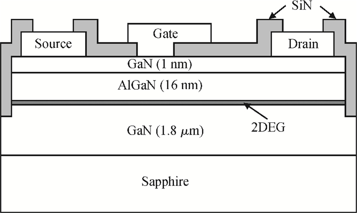
Fig. 1.
The structure of the AlGaN/GaN HEMT device.
SEMICONDUCTOR DEVICES
Chong Wang, Chong Chen, Yunlong He, Xuefeng Zheng, Xiaohua Ma, Jincheng Zhang, Wei Mao and Yue Hao
Corresponding author: Wang Chong, Email:chongw@xidian.edu.cn
Abstract: The breakdown and the current collapse characteristics of high electron mobility transistors (HEMTs) with a low power F-plasma treatment process are investigated. With the increase of F-plasma treatment time, the saturation current decreases, and the threshold voltage shifts to the positive slightly. Through analysis of the Schottky characteristics of the devices with different F-plasma treatment times, it was found that an optimal F-plasma treatment time of 120 s obviously reduced the gate reverse leakage current and improved the breakdown voltage of the devices, but longer F-plasma treatment time than 120 s did not reduce gate reverse leakage current due to plasma damage. The current collapse characteristics of the HEMTs with F-plasma treatment were evaluated by dual pulse measurement at different bias voltages and no obvious deterioration of current collapse were found after low power F-plasma treatment.
Keywords: high electron mobility transistors, AlGaN/GaN, breakdown voltage, current collapse
| [1] |
Kumar V, Lu W, Schwindt R, et al. AlGaN/GaN HEMTs on SiC with fT of over 120 GHz. IEEE Electron Device Lett, 2002, 23(8):455 doi: 10.1109/LED.2002.801303
|
| [2] |
Kumar V, Kim D H, Basu A, et al. 0.25μm self-aligned AlGaN/GaN high electron mobility transistors. IEEE Electron Device Lett, 2008, 29(1):18 doi: 10.1109/LED.2007.911612
|
| [3] |
Koudymov A, Wang C X, Adivarahan V, et al. Power stability of AlGaN/GaN HFETs at 20 W/mm in the pinched-off operation mode. IEEE Electron Device Lett, 2007, 28(1):5 doi: 10.1109/LED.2006.887642
|
| [4] |
Ren Chunjiang, Li Zhonghui, Yu Xuming, et al. Field plated 0.15μm GaN HEMTs for millimeter-wave application. Journal of Semiconductors, 2013, 34(6):064002 doi: 10.1088/1674-4926/34/6/064002
|
| [5] |
Wu Y F, Moore M, Saxler A. 40-W/mm double field-plated GaN HEMTs. Device Research Conference, State College, PA, USA, 2006, 64:151 http://ieeexplore.ieee.org/document/4097579/authors
|
| [6] |
Wang M, Chen K J. Improvement of the off-state breakdown voltage with fluorine ion implantation in AlGaN/GaN HEMTs. IEEE Trans Electron Devices, 2011, 58(2):460 doi: 10.1109/TED.2010.2091958
|
| [7] |
Chu R M, Shen L K, Fichtenbaum N, et al. Plasma treatment for leakage reduction in AlGaN/GaN and GaN Schottky contacts. IEEE Electron Device Lett, 2008, 29(4):297 doi: 10.1109/LED.2008.917814
|
| [8] |
Koudymov A, Shur M S, Simin G, et al. Compact model of current collapse in heterostructure field-effect transistors. IEEE Electron Device Lett, 2007, 28(5):332 doi: 10.1109/LED.2007.895389
|
| [9] |
Chen Wanjun, Zhang Jing, Zhang Bo, et al. Fluorine-plasma surface treatment for gate forward leakage current reduction in AlGaN/GaN HEMTs. Journal of Semiconductors, 2013, 34(2):024003 doi: 10.1088/1674-4926/34/2/024003
|
| [10] |
Karmalkar S, Satyan N, Sathaiya D M. On the resolution of the mechanism for reverse gate leakage in AlGaN/GaN HEMTs. IEEE Electron Device Lett, 2006, 27(2):87 doi: 10.1109/LED.2005.862672
|
| [11] |
Lahbabi M, Ahaitouf A, Fliyou M, et al. Analysis of electroluminescence spectra of silicon and gallium arsenide p-n junctions in avalanche breakdown. Appl Phys Lett, 2004, 95(4):1822 https://works.bepress.com/sherra_kerns/1/
|
| [12] |
Jia S, Cai Y, Wang D, et al. Enhancement-mode AlGaN/GaN HEMTs on silicon substrate. IEEE Trans Electron Devices, 2006, 53(6):1474 doi: 10.1109/TED.2006.873881
|
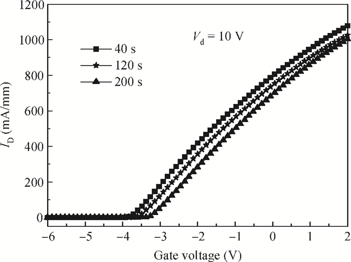
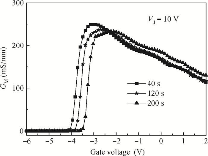
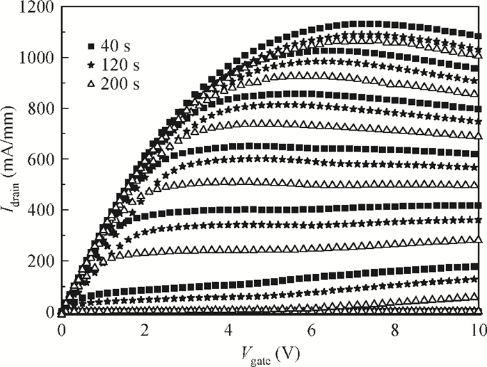
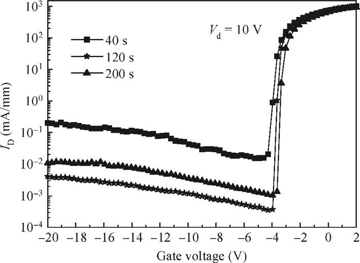
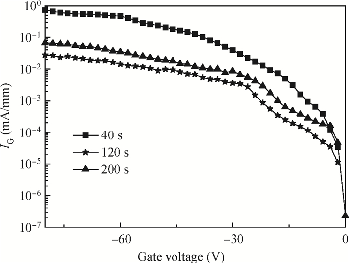
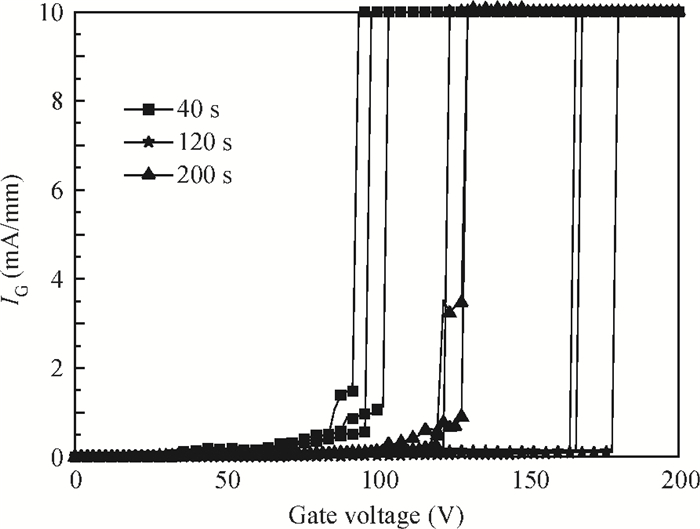
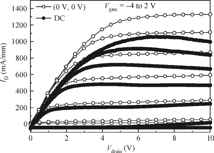
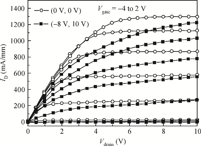
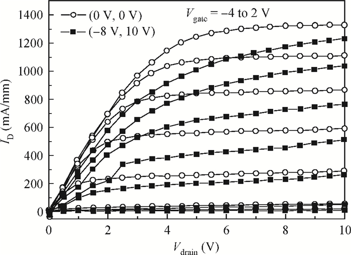
Table 1. Current collapse at different treatment times.

|
| [1] |
Kumar V, Lu W, Schwindt R, et al. AlGaN/GaN HEMTs on SiC with fT of over 120 GHz. IEEE Electron Device Lett, 2002, 23(8):455 doi: 10.1109/LED.2002.801303
|
| [2] |
Kumar V, Kim D H, Basu A, et al. 0.25μm self-aligned AlGaN/GaN high electron mobility transistors. IEEE Electron Device Lett, 2008, 29(1):18 doi: 10.1109/LED.2007.911612
|
| [3] |
Koudymov A, Wang C X, Adivarahan V, et al. Power stability of AlGaN/GaN HFETs at 20 W/mm in the pinched-off operation mode. IEEE Electron Device Lett, 2007, 28(1):5 doi: 10.1109/LED.2006.887642
|
| [4] |
Ren Chunjiang, Li Zhonghui, Yu Xuming, et al. Field plated 0.15μm GaN HEMTs for millimeter-wave application. Journal of Semiconductors, 2013, 34(6):064002 doi: 10.1088/1674-4926/34/6/064002
|
| [5] |
Wu Y F, Moore M, Saxler A. 40-W/mm double field-plated GaN HEMTs. Device Research Conference, State College, PA, USA, 2006, 64:151 http://ieeexplore.ieee.org/document/4097579/authors
|
| [6] |
Wang M, Chen K J. Improvement of the off-state breakdown voltage with fluorine ion implantation in AlGaN/GaN HEMTs. IEEE Trans Electron Devices, 2011, 58(2):460 doi: 10.1109/TED.2010.2091958
|
| [7] |
Chu R M, Shen L K, Fichtenbaum N, et al. Plasma treatment for leakage reduction in AlGaN/GaN and GaN Schottky contacts. IEEE Electron Device Lett, 2008, 29(4):297 doi: 10.1109/LED.2008.917814
|
| [8] |
Koudymov A, Shur M S, Simin G, et al. Compact model of current collapse in heterostructure field-effect transistors. IEEE Electron Device Lett, 2007, 28(5):332 doi: 10.1109/LED.2007.895389
|
| [9] |
Chen Wanjun, Zhang Jing, Zhang Bo, et al. Fluorine-plasma surface treatment for gate forward leakage current reduction in AlGaN/GaN HEMTs. Journal of Semiconductors, 2013, 34(2):024003 doi: 10.1088/1674-4926/34/2/024003
|
| [10] |
Karmalkar S, Satyan N, Sathaiya D M. On the resolution of the mechanism for reverse gate leakage in AlGaN/GaN HEMTs. IEEE Electron Device Lett, 2006, 27(2):87 doi: 10.1109/LED.2005.862672
|
| [11] |
Lahbabi M, Ahaitouf A, Fliyou M, et al. Analysis of electroluminescence spectra of silicon and gallium arsenide p-n junctions in avalanche breakdown. Appl Phys Lett, 2004, 95(4):1822 https://works.bepress.com/sherra_kerns/1/
|
| [12] |
Jia S, Cai Y, Wang D, et al. Enhancement-mode AlGaN/GaN HEMTs on silicon substrate. IEEE Trans Electron Devices, 2006, 53(6):1474 doi: 10.1109/TED.2006.873881
|


Article views: 3499 Times PDF downloads: 52 Times Cited by: 0 Times
Received: 03 June 2013 Revised: 22 August 2013 Online: Published: 01 January 2014
| Citation: |
Chong Wang, Chong Chen, Yunlong He, Xuefeng Zheng, Xiaohua Ma, Jincheng Zhang, Wei Mao, Yue Hao. Breakdown voltage and current collapse of F-plasma treated AlGaN/GaN HEMTs[J]. Journal of Semiconductors, 2014, 35(1): 014008. doi: 10.1088/1674-4926/35/1/014008
****
C Wang, C Chen, Y L He, X F Zheng, X H Ma, J C Zhang, W Mao, Y Hao. Breakdown voltage and current collapse of F-plasma treated AlGaN/GaN HEMTs[J]. J. Semicond., 2014, 35(1): 014008. doi: 10.1088/1674-4926/35/1/014008.

|
| [1] |
Kumar V, Lu W, Schwindt R, et al. AlGaN/GaN HEMTs on SiC with fT of over 120 GHz. IEEE Electron Device Lett, 2002, 23(8):455 doi: 10.1109/LED.2002.801303
|
| [2] |
Kumar V, Kim D H, Basu A, et al. 0.25μm self-aligned AlGaN/GaN high electron mobility transistors. IEEE Electron Device Lett, 2008, 29(1):18 doi: 10.1109/LED.2007.911612
|
| [3] |
Koudymov A, Wang C X, Adivarahan V, et al. Power stability of AlGaN/GaN HFETs at 20 W/mm in the pinched-off operation mode. IEEE Electron Device Lett, 2007, 28(1):5 doi: 10.1109/LED.2006.887642
|
| [4] |
Ren Chunjiang, Li Zhonghui, Yu Xuming, et al. Field plated 0.15μm GaN HEMTs for millimeter-wave application. Journal of Semiconductors, 2013, 34(6):064002 doi: 10.1088/1674-4926/34/6/064002
|
| [5] |
Wu Y F, Moore M, Saxler A. 40-W/mm double field-plated GaN HEMTs. Device Research Conference, State College, PA, USA, 2006, 64:151 http://ieeexplore.ieee.org/document/4097579/authors
|
| [6] |
Wang M, Chen K J. Improvement of the off-state breakdown voltage with fluorine ion implantation in AlGaN/GaN HEMTs. IEEE Trans Electron Devices, 2011, 58(2):460 doi: 10.1109/TED.2010.2091958
|
| [7] |
Chu R M, Shen L K, Fichtenbaum N, et al. Plasma treatment for leakage reduction in AlGaN/GaN and GaN Schottky contacts. IEEE Electron Device Lett, 2008, 29(4):297 doi: 10.1109/LED.2008.917814
|
| [8] |
Koudymov A, Shur M S, Simin G, et al. Compact model of current collapse in heterostructure field-effect transistors. IEEE Electron Device Lett, 2007, 28(5):332 doi: 10.1109/LED.2007.895389
|
| [9] |
Chen Wanjun, Zhang Jing, Zhang Bo, et al. Fluorine-plasma surface treatment for gate forward leakage current reduction in AlGaN/GaN HEMTs. Journal of Semiconductors, 2013, 34(2):024003 doi: 10.1088/1674-4926/34/2/024003
|
| [10] |
Karmalkar S, Satyan N, Sathaiya D M. On the resolution of the mechanism for reverse gate leakage in AlGaN/GaN HEMTs. IEEE Electron Device Lett, 2006, 27(2):87 doi: 10.1109/LED.2005.862672
|
| [11] |
Lahbabi M, Ahaitouf A, Fliyou M, et al. Analysis of electroluminescence spectra of silicon and gallium arsenide p-n junctions in avalanche breakdown. Appl Phys Lett, 2004, 95(4):1822 https://works.bepress.com/sherra_kerns/1/
|
| [12] |
Jia S, Cai Y, Wang D, et al. Enhancement-mode AlGaN/GaN HEMTs on silicon substrate. IEEE Trans Electron Devices, 2006, 53(6):1474 doi: 10.1109/TED.2006.873881
|

 WeChat ID
Journal of Semiconductors © 2017 All Rights Reserved 京ICP备05085259号-2

 DownLoad:

