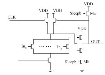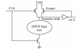
Fig. 1.
Standard n-type domino logic circuit.
SEMICONDUCTOR INTEGRATED CIRCUITS
Huaguo Liang1, Hui Xu2, 3, , Zhengfeng Huang1 and Maoxiang Yi1
Corresponding author: Xu Hui, Email:xuhui@aust.edu.cn
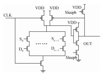
Abstract: NBTI-induced transistor aging has become a prominent factor affecting the reliability of circuits. Reducing leakage consumption is one of the major design goals. Domino logic circuits are applied extensively in high-performance integrated circuits. A circuit technique for mitigating NBTI-induced degradation and reduce standby leakage current is presented in this paper. Two transistors are added to the standard domino circuit to pull both the dynamic node and the output up to VDD, which puts both the keeper and the inverter pMOS transistor into recovery mode in standby mode. Due to the stack effect, leakage current is reduced by the all-0 input vector and the added transistors. Experimental results reveal up to 33% NBTI-induced degradation reduction and up to 79% leakage current reduction.
Keywords: domino logic circuit, negative bias temperature instability, leakage current, standby mode
| [1] |
Kursun V, Friedman E G. Sleep switch dual threshold voltage domino logic with reduced standby leakage current. IEEE Trans Very Large Scale Integration (VLSI) Syst, 2004, 12(5):485 doi: 10.1109/TVLSI.2004.826198
|
| [2] |
Hyungwoo L, Heejung S, Seungho J, et al. Statistical leakage estimation for DRAM circuits. Proc 2nd Asia Symposium on Quality Electronic Design (ASQED), 2010:243
|
| [3] |
Hui X, Huaguo L, Zhengfeng H, et al. An aging tolerant Domino gate. J Circuits Syst, 2012, 17(5):91 http://ieeexplore.ieee.org/document/7494216/
|
| [4] |
Kaffashian M H, Lotfi R, Mafinezhad K, et al. Impact of NBTI on performance of domino logic circuits in nano-scale CMOS. Microelectron J, 2011, (32):1327 doi: 10.1007/978-1-4614-0818-5_6
|
| [5] |
Kaffashian M H, Lotfi R, Mafinezhadand K, et al. An optimization method for NBTI-aware design of Domino logic circuits in nano-scale CMOS. Electron Express, 2011, 81:406 https://www.jstage.jst.go.jp/article/elex/8/19/8_19_1640/_article
|
| [6] |
Yu W, Hong L, Ku H, et al. Temperature-aware NBTI modeling and the impact of input vector control on performance degradation. Proc Design, Automation & Test in Europe Conference & Exhibition, 2007:1 http://www.nsfc.gov.cn/Portals/0/fj/fj20170118_03.xls
|
| [7] |
Feng Chaochao, Chen Xun, Yi Xiaofei, et al. An improved high fan-in Domino circuit for high performance microprocessors. Journal of Semiconductors, 2008, 29(9):1740 http://www.jos.ac.cn/bdtxbcn/ch/reader/view_abstract.aspx?file_no=08011602&flag=1
|
| [8] |
Wang Jinhui, Gong Na, Hou Ligang, et al. Charge self-compensation technology research for low power and high performance Domino circuits. Journal of Semiconductors, 2008, 29(7):1412 http://www.jos.ac.cn/bdtxbcn/ch/reader/view_abstract.aspx?file_no=08010402&flag=1
|
| [9] |
Borkar S. Circuit techniques for subthreshold leakage avoidance, control and tolerance. IEDM Technical Digest, IEEE International Electron Devices Meeting, 2004:421
|
| [10] |
Anis M H, Allam M W, Elmasry M I. Energy-efficient noise-tolerant dynamic styles for scaled-down CMOS and MTCMOS technologies. IEEE Trans Very Large Scale Integration Syst, 2002, 10(2):71 doi: 10.1109/92.994977
|
| [11] |
Song J, Yinhe H, Huawei L, et al. On predicting circuit aging via considering actual workload. Journal of Computer-Aided Design & Computer Graphics, 2010, (12):2242 http://en.cnki.com.cn/Article_en/CJFDTOTAL-JSJF201012028.htm
|
| [12] |
Wu K C, Marculescu D. Joint logic restructuring and pin reordering against NBTI-induced performance degradation. Proc Design, Automation & Test in Europe Conference & Exhibition, 2009:75 https://core.ac.uk/display/21196869
|
| [13] |
Wang J, Wu W, Lei Z, et al. Power and delay estimation for dynamic OR gates with header and footer transistor based on wavelet neural networks. 10th International Conference on Ultimate Integration of Silicon, 2009:241 doi: 10.1007/978-3-319-18802-7_3
|
| [14] |
Hua C H, Hwang W, Chen C K. Noise-tolerant XOR-based conditional keeper for high fan-in dynamic circuits. IEEE International Symposium on Circuits and Systems, 2005:444
|
| [15] |
Bhardwaj S, Wenping W, Vattikonda R, et al. Predictive modeling of the NBTI effect for reliable design. Proc Custom Integrated Circuits Conference, 2006:189 doi: 10.1007/978-3-642-36157-9_16
|
| [16] |
Wang W, Wei Z, Yang S, et al. An efficient method to identify critical gates under circuit aging. IEEE/ACM International Conference on Computer-Aided Design, 2007:735 doi: 10.1007/s10836-013-5358-z
|
| [17] |
Wu K C, Marculescu D. Aging-aware timing analysis and optimization considering path sensitization. Proc Design, Automation & Test in Europe Conference & Exhibition (DATE), 2011, 2011:1 https://www.computer.org/csdl/proceedings/date/2011/4208/00/05763249.pdf
|
| [18] |
Predictive technology model (PTM). http://www.eas.asu.edu/ptm/
|
| [19] |
Wang Y, Chen X, Wang W, et al. Leakage power and circuit aging cooptimization by gate replacement techniques. IEEE Trans Very Large Scale Integration Syst, 2011, 19(4):615 doi: 10.1109/TVLSI.2009.2037637
|
| [20] |
Siddiqua T, Gurumurthi S. Recovery boosting:a technique to enhance NBTI recovery in SRAM arrays. IEEE Computer Society Annual Symposium on VLSI (ISVLSI), 2010:393 http://citeseerx.ist.psu.edu/viewdoc/summary?doi=10.1.1.294.9741
|
| [21] |
Vattikonda R, Wang W, Yu C. Modeling and minimization of PMOS NBTI effect for robust nanometer design. 43rd ACM/IEEE Design Automation Conference, 2006:1047 https://asu.pure.elsevier.com/en/publications/modeling-and-minimization-of-pmos-nbti-effect-for-robust-nanomete
|
| [22] |
Wang Y, Chen X, Wang W, et al. On the efficacy of input Vector control to mitigate NBTI effects and leakage power. International Symposium on Quality of Electronic Design, ISQED, 2009:19
|
| [23] |
Bild D R, Bok G E, Dick R P. Minimization of NBTI performance degradation using internal node control. Proc Design, Automation & Test in Europe Conference & Exhibition, 2009:148
|
| [24] |
Lin Y, Gang Q. A combined gate replacement and input vector control approach for leakage current reduction. IEEE Trans Very Large Scale Integration (VLSI) Syst, 2006, 14(2):173 doi: 10.1109/TVLSI.2005.863747
|
| [25] |
Paul B C, Kunhyuk K, Kufluoglu H, et al. Temporal performance degradation under NBTI:estimation and design for improved reliability of nanoscale circuits. Proc Design, Automation and Test in Europe, 2006:780 doi: 10.1145/1131703
|
| [26] |
Gong N, Tang G, Wang J, et al. Novel adaptive keeper LBL technique for low power and high performance register files. IEEE International SOC Conference (SOCC), 2011:30 http://ieeexplore.ieee.org/xpl/mostRecentIssue.jsp?punumber=6076821
|
| [27] |
Eriksson H, Larsson-Edefors P, Henriksson T, et al. Full-custom vs. standard-cell design flow:an adder case study. Proceedings of the Asia and South Pacific Design Automation Conference, Kitakyushu, Japan, 2003:507
|
| [28] |
Eleyan N N, Ken L, Kamal M, et al. Semi-custom design flow:leveraging place and route tools in custom circuit design. IEEE International Conference on IC Design and Technology, 2009:143
|
| [29] |
Lin I C, Lin C H, Li K H. Leakage and aging optimization using transmission gate-based technique. IEEE Trans Computer-Aided Design of Integrated Circuits and Systems, 2013, 32(1):87 doi: 10.1109/TCAD.2012.2214478
|
| [30] |
Abdollahi A, Fallah F, Pedram M. Leakage current reduction in CMOS VLSI circuits by input vector control. IEEE Trans Very Large Scale Integration (VLSI) Syst, 2004, 12(2):140 doi: 10.1109/TVLSI.2003.821546
|
| [31] |
Khandelwal V, Srivastava A. Leakage control through fine-grained placement and sizing of sleep transistors. IEEE Trans Computer-Aided Design of Integrated Circuits and Systems, 2007, 26(7):1246 doi: 10.1109/TCAD.2006.888282
|
Table 1. Short-term cycle-by-cycle model of degradation.

|
Table 2. Degradation of different circuits.

|
Table 3. Area overhead.

|
Table 4. Normalized dynamic power overhead.

|
| [1] |
Kursun V, Friedman E G. Sleep switch dual threshold voltage domino logic with reduced standby leakage current. IEEE Trans Very Large Scale Integration (VLSI) Syst, 2004, 12(5):485 doi: 10.1109/TVLSI.2004.826198
|
| [2] |
Hyungwoo L, Heejung S, Seungho J, et al. Statistical leakage estimation for DRAM circuits. Proc 2nd Asia Symposium on Quality Electronic Design (ASQED), 2010:243
|
| [3] |
Hui X, Huaguo L, Zhengfeng H, et al. An aging tolerant Domino gate. J Circuits Syst, 2012, 17(5):91 http://ieeexplore.ieee.org/document/7494216/
|
| [4] |
Kaffashian M H, Lotfi R, Mafinezhad K, et al. Impact of NBTI on performance of domino logic circuits in nano-scale CMOS. Microelectron J, 2011, (32):1327 doi: 10.1007/978-1-4614-0818-5_6
|
| [5] |
Kaffashian M H, Lotfi R, Mafinezhadand K, et al. An optimization method for NBTI-aware design of Domino logic circuits in nano-scale CMOS. Electron Express, 2011, 81:406 https://www.jstage.jst.go.jp/article/elex/8/19/8_19_1640/_article
|
| [6] |
Yu W, Hong L, Ku H, et al. Temperature-aware NBTI modeling and the impact of input vector control on performance degradation. Proc Design, Automation & Test in Europe Conference & Exhibition, 2007:1 http://www.nsfc.gov.cn/Portals/0/fj/fj20170118_03.xls
|
| [7] |
Feng Chaochao, Chen Xun, Yi Xiaofei, et al. An improved high fan-in Domino circuit for high performance microprocessors. Journal of Semiconductors, 2008, 29(9):1740 http://www.jos.ac.cn/bdtxbcn/ch/reader/view_abstract.aspx?file_no=08011602&flag=1
|
| [8] |
Wang Jinhui, Gong Na, Hou Ligang, et al. Charge self-compensation technology research for low power and high performance Domino circuits. Journal of Semiconductors, 2008, 29(7):1412 http://www.jos.ac.cn/bdtxbcn/ch/reader/view_abstract.aspx?file_no=08010402&flag=1
|
| [9] |
Borkar S. Circuit techniques for subthreshold leakage avoidance, control and tolerance. IEDM Technical Digest, IEEE International Electron Devices Meeting, 2004:421
|
| [10] |
Anis M H, Allam M W, Elmasry M I. Energy-efficient noise-tolerant dynamic styles for scaled-down CMOS and MTCMOS technologies. IEEE Trans Very Large Scale Integration Syst, 2002, 10(2):71 doi: 10.1109/92.994977
|
| [11] |
Song J, Yinhe H, Huawei L, et al. On predicting circuit aging via considering actual workload. Journal of Computer-Aided Design & Computer Graphics, 2010, (12):2242 http://en.cnki.com.cn/Article_en/CJFDTOTAL-JSJF201012028.htm
|
| [12] |
Wu K C, Marculescu D. Joint logic restructuring and pin reordering against NBTI-induced performance degradation. Proc Design, Automation & Test in Europe Conference & Exhibition, 2009:75 https://core.ac.uk/display/21196869
|
| [13] |
Wang J, Wu W, Lei Z, et al. Power and delay estimation for dynamic OR gates with header and footer transistor based on wavelet neural networks. 10th International Conference on Ultimate Integration of Silicon, 2009:241 doi: 10.1007/978-3-319-18802-7_3
|
| [14] |
Hua C H, Hwang W, Chen C K. Noise-tolerant XOR-based conditional keeper for high fan-in dynamic circuits. IEEE International Symposium on Circuits and Systems, 2005:444
|
| [15] |
Bhardwaj S, Wenping W, Vattikonda R, et al. Predictive modeling of the NBTI effect for reliable design. Proc Custom Integrated Circuits Conference, 2006:189 doi: 10.1007/978-3-642-36157-9_16
|
| [16] |
Wang W, Wei Z, Yang S, et al. An efficient method to identify critical gates under circuit aging. IEEE/ACM International Conference on Computer-Aided Design, 2007:735 doi: 10.1007/s10836-013-5358-z
|
| [17] |
Wu K C, Marculescu D. Aging-aware timing analysis and optimization considering path sensitization. Proc Design, Automation & Test in Europe Conference & Exhibition (DATE), 2011, 2011:1 https://www.computer.org/csdl/proceedings/date/2011/4208/00/05763249.pdf
|
| [18] |
Predictive technology model (PTM). http://www.eas.asu.edu/ptm/
|
| [19] |
Wang Y, Chen X, Wang W, et al. Leakage power and circuit aging cooptimization by gate replacement techniques. IEEE Trans Very Large Scale Integration Syst, 2011, 19(4):615 doi: 10.1109/TVLSI.2009.2037637
|
| [20] |
Siddiqua T, Gurumurthi S. Recovery boosting:a technique to enhance NBTI recovery in SRAM arrays. IEEE Computer Society Annual Symposium on VLSI (ISVLSI), 2010:393 http://citeseerx.ist.psu.edu/viewdoc/summary?doi=10.1.1.294.9741
|
| [21] |
Vattikonda R, Wang W, Yu C. Modeling and minimization of PMOS NBTI effect for robust nanometer design. 43rd ACM/IEEE Design Automation Conference, 2006:1047 https://asu.pure.elsevier.com/en/publications/modeling-and-minimization-of-pmos-nbti-effect-for-robust-nanomete
|
| [22] |
Wang Y, Chen X, Wang W, et al. On the efficacy of input Vector control to mitigate NBTI effects and leakage power. International Symposium on Quality of Electronic Design, ISQED, 2009:19
|
| [23] |
Bild D R, Bok G E, Dick R P. Minimization of NBTI performance degradation using internal node control. Proc Design, Automation & Test in Europe Conference & Exhibition, 2009:148
|
| [24] |
Lin Y, Gang Q. A combined gate replacement and input vector control approach for leakage current reduction. IEEE Trans Very Large Scale Integration (VLSI) Syst, 2006, 14(2):173 doi: 10.1109/TVLSI.2005.863747
|
| [25] |
Paul B C, Kunhyuk K, Kufluoglu H, et al. Temporal performance degradation under NBTI:estimation and design for improved reliability of nanoscale circuits. Proc Design, Automation and Test in Europe, 2006:780 doi: 10.1145/1131703
|
| [26] |
Gong N, Tang G, Wang J, et al. Novel adaptive keeper LBL technique for low power and high performance register files. IEEE International SOC Conference (SOCC), 2011:30 http://ieeexplore.ieee.org/xpl/mostRecentIssue.jsp?punumber=6076821
|
| [27] |
Eriksson H, Larsson-Edefors P, Henriksson T, et al. Full-custom vs. standard-cell design flow:an adder case study. Proceedings of the Asia and South Pacific Design Automation Conference, Kitakyushu, Japan, 2003:507
|
| [28] |
Eleyan N N, Ken L, Kamal M, et al. Semi-custom design flow:leveraging place and route tools in custom circuit design. IEEE International Conference on IC Design and Technology, 2009:143
|
| [29] |
Lin I C, Lin C H, Li K H. Leakage and aging optimization using transmission gate-based technique. IEEE Trans Computer-Aided Design of Integrated Circuits and Systems, 2013, 32(1):87 doi: 10.1109/TCAD.2012.2214478
|
| [30] |
Abdollahi A, Fallah F, Pedram M. Leakage current reduction in CMOS VLSI circuits by input vector control. IEEE Trans Very Large Scale Integration (VLSI) Syst, 2004, 12(2):140 doi: 10.1109/TVLSI.2003.821546
|
| [31] |
Khandelwal V, Srivastava A. Leakage control through fine-grained placement and sizing of sleep transistors. IEEE Trans Computer-Aided Design of Integrated Circuits and Systems, 2007, 26(7):1246 doi: 10.1109/TCAD.2006.888282
|


Article views: 2862 Times PDF downloads: 19 Times Cited by: 0 Times
Received: 22 May 2013 Revised: 24 July 2013 Online: Published: 01 January 2014
| Citation: |
Huaguo Liang, Hui Xu, Zhengfeng Huang, Maoxiang Yi. A low-leakage and NBTI-mitigated N-type domino logic[J]. Journal of Semiconductors, 2014, 35(1): 015009. doi: 10.1088/1674-4926/35/1/015009
****
H G Liang, H Xu, Z F Huang, M X Yi. A low-leakage and NBTI-mitigated N-type domino logic[J]. J. Semicond., 2014, 35(1): 015009. doi: 10.1088/1674-4926/35/1/015009.

|
| [1] |
Kursun V, Friedman E G. Sleep switch dual threshold voltage domino logic with reduced standby leakage current. IEEE Trans Very Large Scale Integration (VLSI) Syst, 2004, 12(5):485 doi: 10.1109/TVLSI.2004.826198
|
| [2] |
Hyungwoo L, Heejung S, Seungho J, et al. Statistical leakage estimation for DRAM circuits. Proc 2nd Asia Symposium on Quality Electronic Design (ASQED), 2010:243
|
| [3] |
Hui X, Huaguo L, Zhengfeng H, et al. An aging tolerant Domino gate. J Circuits Syst, 2012, 17(5):91 http://ieeexplore.ieee.org/document/7494216/
|
| [4] |
Kaffashian M H, Lotfi R, Mafinezhad K, et al. Impact of NBTI on performance of domino logic circuits in nano-scale CMOS. Microelectron J, 2011, (32):1327 doi: 10.1007/978-1-4614-0818-5_6
|
| [5] |
Kaffashian M H, Lotfi R, Mafinezhadand K, et al. An optimization method for NBTI-aware design of Domino logic circuits in nano-scale CMOS. Electron Express, 2011, 81:406 https://www.jstage.jst.go.jp/article/elex/8/19/8_19_1640/_article
|
| [6] |
Yu W, Hong L, Ku H, et al. Temperature-aware NBTI modeling and the impact of input vector control on performance degradation. Proc Design, Automation & Test in Europe Conference & Exhibition, 2007:1 http://www.nsfc.gov.cn/Portals/0/fj/fj20170118_03.xls
|
| [7] |
Feng Chaochao, Chen Xun, Yi Xiaofei, et al. An improved high fan-in Domino circuit for high performance microprocessors. Journal of Semiconductors, 2008, 29(9):1740 http://www.jos.ac.cn/bdtxbcn/ch/reader/view_abstract.aspx?file_no=08011602&flag=1
|
| [8] |
Wang Jinhui, Gong Na, Hou Ligang, et al. Charge self-compensation technology research for low power and high performance Domino circuits. Journal of Semiconductors, 2008, 29(7):1412 http://www.jos.ac.cn/bdtxbcn/ch/reader/view_abstract.aspx?file_no=08010402&flag=1
|
| [9] |
Borkar S. Circuit techniques for subthreshold leakage avoidance, control and tolerance. IEDM Technical Digest, IEEE International Electron Devices Meeting, 2004:421
|
| [10] |
Anis M H, Allam M W, Elmasry M I. Energy-efficient noise-tolerant dynamic styles for scaled-down CMOS and MTCMOS technologies. IEEE Trans Very Large Scale Integration Syst, 2002, 10(2):71 doi: 10.1109/92.994977
|
| [11] |
Song J, Yinhe H, Huawei L, et al. On predicting circuit aging via considering actual workload. Journal of Computer-Aided Design & Computer Graphics, 2010, (12):2242 http://en.cnki.com.cn/Article_en/CJFDTOTAL-JSJF201012028.htm
|
| [12] |
Wu K C, Marculescu D. Joint logic restructuring and pin reordering against NBTI-induced performance degradation. Proc Design, Automation & Test in Europe Conference & Exhibition, 2009:75 https://core.ac.uk/display/21196869
|
| [13] |
Wang J, Wu W, Lei Z, et al. Power and delay estimation for dynamic OR gates with header and footer transistor based on wavelet neural networks. 10th International Conference on Ultimate Integration of Silicon, 2009:241 doi: 10.1007/978-3-319-18802-7_3
|
| [14] |
Hua C H, Hwang W, Chen C K. Noise-tolerant XOR-based conditional keeper for high fan-in dynamic circuits. IEEE International Symposium on Circuits and Systems, 2005:444
|
| [15] |
Bhardwaj S, Wenping W, Vattikonda R, et al. Predictive modeling of the NBTI effect for reliable design. Proc Custom Integrated Circuits Conference, 2006:189 doi: 10.1007/978-3-642-36157-9_16
|
| [16] |
Wang W, Wei Z, Yang S, et al. An efficient method to identify critical gates under circuit aging. IEEE/ACM International Conference on Computer-Aided Design, 2007:735 doi: 10.1007/s10836-013-5358-z
|
| [17] |
Wu K C, Marculescu D. Aging-aware timing analysis and optimization considering path sensitization. Proc Design, Automation & Test in Europe Conference & Exhibition (DATE), 2011, 2011:1 https://www.computer.org/csdl/proceedings/date/2011/4208/00/05763249.pdf
|
| [18] |
Predictive technology model (PTM). http://www.eas.asu.edu/ptm/
|
| [19] |
Wang Y, Chen X, Wang W, et al. Leakage power and circuit aging cooptimization by gate replacement techniques. IEEE Trans Very Large Scale Integration Syst, 2011, 19(4):615 doi: 10.1109/TVLSI.2009.2037637
|
| [20] |
Siddiqua T, Gurumurthi S. Recovery boosting:a technique to enhance NBTI recovery in SRAM arrays. IEEE Computer Society Annual Symposium on VLSI (ISVLSI), 2010:393 http://citeseerx.ist.psu.edu/viewdoc/summary?doi=10.1.1.294.9741
|
| [21] |
Vattikonda R, Wang W, Yu C. Modeling and minimization of PMOS NBTI effect for robust nanometer design. 43rd ACM/IEEE Design Automation Conference, 2006:1047 https://asu.pure.elsevier.com/en/publications/modeling-and-minimization-of-pmos-nbti-effect-for-robust-nanomete
|
| [22] |
Wang Y, Chen X, Wang W, et al. On the efficacy of input Vector control to mitigate NBTI effects and leakage power. International Symposium on Quality of Electronic Design, ISQED, 2009:19
|
| [23] |
Bild D R, Bok G E, Dick R P. Minimization of NBTI performance degradation using internal node control. Proc Design, Automation & Test in Europe Conference & Exhibition, 2009:148
|
| [24] |
Lin Y, Gang Q. A combined gate replacement and input vector control approach for leakage current reduction. IEEE Trans Very Large Scale Integration (VLSI) Syst, 2006, 14(2):173 doi: 10.1109/TVLSI.2005.863747
|
| [25] |
Paul B C, Kunhyuk K, Kufluoglu H, et al. Temporal performance degradation under NBTI:estimation and design for improved reliability of nanoscale circuits. Proc Design, Automation and Test in Europe, 2006:780 doi: 10.1145/1131703
|
| [26] |
Gong N, Tang G, Wang J, et al. Novel adaptive keeper LBL technique for low power and high performance register files. IEEE International SOC Conference (SOCC), 2011:30 http://ieeexplore.ieee.org/xpl/mostRecentIssue.jsp?punumber=6076821
|
| [27] |
Eriksson H, Larsson-Edefors P, Henriksson T, et al. Full-custom vs. standard-cell design flow:an adder case study. Proceedings of the Asia and South Pacific Design Automation Conference, Kitakyushu, Japan, 2003:507
|
| [28] |
Eleyan N N, Ken L, Kamal M, et al. Semi-custom design flow:leveraging place and route tools in custom circuit design. IEEE International Conference on IC Design and Technology, 2009:143
|
| [29] |
Lin I C, Lin C H, Li K H. Leakage and aging optimization using transmission gate-based technique. IEEE Trans Computer-Aided Design of Integrated Circuits and Systems, 2013, 32(1):87 doi: 10.1109/TCAD.2012.2214478
|
| [30] |
Abdollahi A, Fallah F, Pedram M. Leakage current reduction in CMOS VLSI circuits by input vector control. IEEE Trans Very Large Scale Integration (VLSI) Syst, 2004, 12(2):140 doi: 10.1109/TVLSI.2003.821546
|
| [31] |
Khandelwal V, Srivastava A. Leakage control through fine-grained placement and sizing of sleep transistors. IEEE Trans Computer-Aided Design of Integrated Circuits and Systems, 2007, 26(7):1246 doi: 10.1109/TCAD.2006.888282
|

 WeChat ID
Journal of Semiconductors © 2017 All Rights Reserved 京ICP备05085259号-2

 DownLoad: