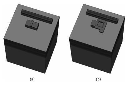
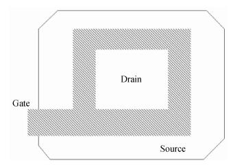
J. Semicond. > 2014, Volume 35 > Issue 1 > 015010

SEMICONDUCTOR INTEGRATED CIRCUITS

A 130 nm radiation hardened flip-flop with an annular gate and a C-element

Lei Wang, Jianhua Jiang, Yiming Xiang and Yumei Zhou

+ Author Affiliations

 Corresponding author: Wang Lei, Email:wanglei3@ime.ac.cn

DOI: 10.1088/1674-4926/35/1/015010

PDF

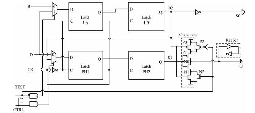
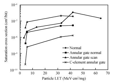
Abstract: This paper presents a radiation hardened flip-flop with an annular gate and a Muller C-element. The proposed cell has multiple working modes which can be used in different situations. Each part of the cell can be verified easily and completely by using different modes. This cell has been designed under an SMIC 0.13 μm process and 3-D simulated by using Synopsys TCAD. Heavy-ion testing has been done on the cell and its counterparts. The test results demonstrate that the presented cell reduces the cell's saturation cross section by approximately two orders of magnitude with little penalty on performance.

Key words: SEUflip-flopannular gateC-element

Stimulated emission and lasing of GaN-based laser diodes (LDs) were reported at 1995[1] and 1996[2], right after the breakthrough of p-type doping[35], material quality[6] and the invention of high-brightness GaN-based LEDs[7, 8]. However, it took much longer time for GaN-based LDs to achieve high power, high wall plug efficiency, and long lifetime. Until 2019, Nichia reported blue LDs with these performances[9], which open wide applications with GaN-based blue LDs.

In the past 5 years, various organizations have reported GaN-based blue LDs with high output power. Osram reported 453 nm blue LDs with wall plug efficiency of 42% at 2.2 W and output power of 5 W at 3 A[10]. Institute of Semiconductors reported 442 nm blue LDs with output power of 6 W at 5 A[11]. Suzhou Institute of Nano-tech and Nano-bionics reported 442 nm blue LDs with output power of 7.5 W at 6 A[12]. Tsinghua University and Anhui GaN Semiconductor achieved a maximum output power of 15 W and the wall plug efficiency of 38% under pulse operation conditions[13]. Nichia reported 455 nm blue LDs with output power of 5.99 W, wall plug efficiency of 52.4% at 3 A, and lifetime more than 30 000 h[14], which is only reported with long lifetime.

Our group reported the first high power blue GaN-based LD and the first green GaN-based LD in China[1517]. We then greatly improved green LD performance by using new structure with ITO cladding layer[18]. UCSB also reported GaN-based LDs using ITO as cladding layer[19], with the device performance only comparable to conventional ones, which could be caused by the problems of high contact resistance and ITO absorption. In this article, we report GaN-based blue laser diodes with ITO cladding layer with reduced contact resistance and absorption coefficient. Output power of 5 W and wall plug efficiency of 41% have achieved at operation current of 3 A. Moreover, lifetime over 20 000 h has been achieved for LDs aged at 60 °C case temperature.

Schematic LD layer structure is shown in Fig. 1, where hybrid GaN-based LD structure use ITO layer to replace part of conventional p-AlGaN cladding layer as a cladding layer and metal p-electrode, which has several advantages over conventional p-AlGaN cladding layer, such as much lower resistance, better optical confinement, lower internal loss, and no thermal budget on InGaN QWs[18]. Because the refractive index of ITO is much lower than that of the p-AlGaN cladding layer, it can provide more sufficient optical confinement. Meanwhile, the temperature to deposit ITO can be around 300 °C or even room temperature, therefore reduce the thermal budget imposed on InGaN QWs and thermal degradation of InGaN QWs. Moreover, the absorption coefficient of ITO is 2 orders of magnitude lower than that of metal, which means the internal loss of hybrid GaN-based LDs with ITO layer can be lower.

Fig. 1.  (Color online) The schematic layer structure of conventional and hybrid GaN-based LDs.

We simulated and compared conventional blue LDs and hybrid blue LDs with ITO layer by the transfer matrix method[20]. The Internal loss as a function of p-AlGaN cladding layer thickness for conventional and hybrid LDs is shown in Fig. 2. In regard to the conventional LDs, when the p-AlGaN cladding layer thickness decreases, the internal loss has a quick increase which results from the significant increase of the absorption in metal p-electrode. As for the hybrid ITO LDs, the internal loss decreases at 300 nm, on the contrary, and then increases slightly. Our internal loss for hybrid LDs is almost one order of magnitude lower than that reported by UCSB group[19].

Fig. 2.  (Color online) Internal loss as a function of p-AlGaN cladding layer thickness for conventional and hybrid LDs.

The LD epitaxial structure with p-AlGaN cladding layers of 300 nm was grown by metal−organic chemical vapor deposition (MOCVD) on c-plane GaN substrates. In order to achieve high power, high wall plug efficiency and long lifetime GaN-based blue LDs, we have optimized the crystalline quality of LD structure, the structure of the LDs, the manufacturing process, and the heat dissipation of p-down packaging[12, 2124].

The blue LDs with a ridge width of 45 μm and a cavity length of 1200 μm were fabricated and the LD characteristics were measured under continuous conditions at room temperature. The typical power−current−voltage (PIV) curves for optimized hybrid GaN-based LDs with ITO cladding layer are shown in Fig. 3(a), the threshold current density is 0.7 kA/cm2, and the slope efficiency is 1.9 W/A. The output power of 5 W and wall plug efficiency of 41% have been achieved at operation current of 3 A. And the lasing wavelength is 450 nm as shown in Fig. 3(b).

Fig. 3.  (Color online) (a) PIV curves, efficiency curve, and (b) lasing spectra of optimized hybrid GaN-based LDs with ITO cladding layer.

We also measured the high-temperature characteristics of the optimized hybrid GaN-based LDs with ITO cladding layer. The PIV curves of blue LDs at 60 °C are shown in Fig. 4(a), the threshold current density increases to 1 kA/cm2, and the slope efficiency drops to 1.76 W/A. The output power is 4.3 W at the current of 3 A. Meanwhile, the aging test was performed at operation current of 3 A and 60 °C case temperature. The output power slightly decreases after more than 1000 h of aging, and the extrapolated high-temperature lifetime exceeded 20 000 h, which is shown in Fig. 4(b).

Fig. 4.  (Color online) (a) PIV curves and (b) aging curves of optimized hybrid GaN-based LDs with ITO cladding layer at 60 °C case temperature.

In summary, hybrid GaN-based blue LDs with ITO cladding layer were developed. Output power of 5 W and wall plug efficiency of 41% have been achieved at operation current of 3 A. Moreover, lifetime over 20 000 h has been achieved for LDs aged at 60 °C case temperature.

This work was supported by the Natural Science Foundation of Jiangsu Province (Grant. BK20232042).


[1]
Petersen E. Single event effects in aerospace. Wiley-IEEE Press, 2010 http://www.wiley.com/WileyCDA/WileyTitle/productCd-1118084314.html
[2]
Nicolaidis M. Design for soft error mitigation. IEEE Trans Device Mater Reliab, 2005, 5(3):405 doi: 10.1109/TDMR.2005.855790
[3]
Gan Xuewen, Wang Xushe, Zhang Xing. Analysis of threshold voltage decreasing for double-gate and surrounding-gate MOSFET's. Chinese Journal of Semiconductors, 2001, 22(12):1581 http://www.oalib.com/paper/1520674
[4]
Mitra S, Seifert N, Zhang M, et al. Robust system design with built-in soft-error resilience. Computer, 2005, 38(2):43 doi: 10.1109/MC.2005.70
[5]
Mitra S, Zhang M, Seifert N, et al. Built-in soft error resilience for robust system design. IEEE International Conference on Integrated Circuit Design and Technology, 2007 http://web.stanford.edu/class/ee386/
[6]
Uemura T, Tosaka Y, Matsuyama H, et al. Robust flip-flop circuit against soft errors for combinational and sequential logic circuits. Jpn J Appl Phys, 2009, 48:04C070 http://adsabs.harvard.edu/abs/2009JaJAP..48dC070U
[7]
Mitra S. Robust system design. 23rd International Conference on VLSI Design, 2010:434
Fig. 1.  Annular gate transistor.

Fig. 2.  C-element and its keeper.

Fig. 3.  Schematic of the proposed flip–flop.

Fig. 4.  3-D modeled transistor.

Fig. 5.  The EVD of the different transistors.

Fig. 6.  Layout implementation of the proposed flip–flop.

Fig. 7.  The chips using an annular gate library.

Fig. 8.  The chips using a direct gate library.

Fig. 9.  The chips using an annular gate library.

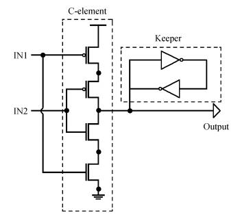
Table 1.   Truth table of C-element.

Table 2.   Flip–flop mode list.

Table 3.   Charges generated from SEE pulses.

[1]
Petersen E. Single event effects in aerospace. Wiley-IEEE Press, 2010 http://www.wiley.com/WileyCDA/WileyTitle/productCd-1118084314.html
[2]
Nicolaidis M. Design for soft error mitigation. IEEE Trans Device Mater Reliab, 2005, 5(3):405 doi: 10.1109/TDMR.2005.855790
[3]
Gan Xuewen, Wang Xushe, Zhang Xing. Analysis of threshold voltage decreasing for double-gate and surrounding-gate MOSFET's. Chinese Journal of Semiconductors, 2001, 22(12):1581 http://www.oalib.com/paper/1520674
[4]
Mitra S, Seifert N, Zhang M, et al. Robust system design with built-in soft-error resilience. Computer, 2005, 38(2):43 doi: 10.1109/MC.2005.70
[5]
Mitra S, Zhang M, Seifert N, et al. Built-in soft error resilience for robust system design. IEEE International Conference on Integrated Circuit Design and Technology, 2007 http://web.stanford.edu/class/ee386/
[6]
Uemura T, Tosaka Y, Matsuyama H, et al. Robust flip-flop circuit against soft errors for combinational and sequential logic circuits. Jpn J Appl Phys, 2009, 48:04C070 http://adsabs.harvard.edu/abs/2009JaJAP..48dC070U
[7]
Mitra S. Robust system design. 23rd International Conference on VLSI Design, 2010:434
1

Dual material gate doping-less tunnel FET with hetero gate dielectric for enhancement of analog/RF performance

Sunny Anand, R.K. Sarin

Journal of Semiconductors, 2017, 38(2): 024001. doi: 10.1088/1674-4926/38/2/024001

2

A high-conductivity insulated gate bipolar transistor with Schottky hole barrier contact

Mengxuan Jiang, Z. John Shen, Jun Wang, Xin Yin, Zhikang Shuai, et al.

Journal of Semiconductors, 2016, 37(2): 024011. doi: 10.1088/1674-4926/37/2/024011

3

Detection of lead ions with AlGaAs/InGaAs pseudomorphic high electron mobility transistor

Jiqiang Niu, Yang Zhang, Min Guan, Chengyan Wang, Lijie Cui, et al.

Journal of Semiconductors, 2016, 37(11): 114003. doi: 10.1088/1674-4926/37/11/114003

4

Single event soft error in advanced integrated circuit

Yuanfu Zhao, Suge Yue, Xinyuan Zhao, Shijin Lu, Qiang Bian, et al.

Journal of Semiconductors, 2015, 36(11): 111001. doi: 10.1088/1674-4926/36/11/111001

5

Simulation and research on a 4T-cell based duplication redundancy SRAM for SEU radiation hardening

Xinhong Hong, Liyang Pan, Wendi Zhang, Dongmei Ji, Dong Wu, et al.

Journal of Semiconductors, 2015, 36(11): 114003. doi: 10.1088/1674-4926/36/11/114003

6

A trench accumulation layer controlled insulated gate bipolar transistor with a semi-SJ structure

Binghua Li, Frank X. C. Jiang, Zhigui Li, Xinnan Lin

Journal of Semiconductors, 2013, 34(12): 124001. doi: 10.1088/1674-4926/34/12/124001

7

A dual redundancy radiation-hardened flip-flop based on a C-element in a 65 nm process

Gang Chen, Bo Gao, Min Gong

Journal of Semiconductors, 2013, 34(9): 095012. doi: 10.1088/1674-4926/34/9/095012

8

Gate leakage current reduction in IP3 SRAM cells at 45 nm CMOS technology for multimedia applications

R. K. Singh, Neeraj Kr. Shukla, Manisha Pattanaik

Journal of Semiconductors, 2012, 33(5): 055001. doi: 10.1088/1674-4926/33/5/055001

9

Low power digitally controlled oscillator designs with a novel 3-transistor XNOR gate

Manoj Kumar, Sandeep K. Arya, Sujata Pandey

Journal of Semiconductors, 2012, 33(3): 035001. doi: 10.1088/1674-4926/33/3/035001

10

Monolithically integrated enhancement/depletion-mode AlGaN/GaN HEMT D flip-flop using fluorine plasma treatment

Xie Yuanbin, Quan Si, Ma Xiaohua, Zhang Jincheng, Li Qingmin, et al.

Journal of Semiconductors, 2011, 32(6): 065001. doi: 10.1088/1674-4926/32/6/065001

11

Novel SEU hardened PD SOI SRAM cell

Xie Chengmin, Wang Zhongfang, Wang Xihu, Wu Longsheng, Liu Youbao, et al.

Journal of Semiconductors, 2011, 32(11): 115017. doi: 10.1088/1674-4926/32/11/115017

12

Erase voltage impact on 0.18 μm triple self-aligned split-gate flash memory endurance

Dong Yaoqi, Kong Weiran, Nhan Do, Wang Shiuh-Luen, Lee Gabriel, et al.

Journal of Semiconductors, 2010, 31(6): 064012. doi: 10.1088/1674-4926/31/6/064012

13

The Bipolar Field-Effect Transistor: VIII. Longitudinal Gradient of Longitudinal Electric Field (Two-MOS-Gates on Pure-Base)

Jie Binbin, Sah Chihtang

Journal of Semiconductors, 2010, 31(7): 071001. doi: 10.1088/1674-4926/31/7/071001

14

The Bipolar Field-Effect Transistor: VII. The Unipolar Current Mode for Analog-RF Operation (Two-MOS-Gates on Pure-Base)

Jie Binbin, Sah Chih-Tang

Journal of Semiconductors, 2009, 30(3): 031001. doi: 10.1088/1674-4926/30/3/031001

15

Structural and electrical characteristics of lanthanum oxide gate dielectric film on GaAs pHEMT technology

Wu Chia-Song, Liu Hsing-Chung

Journal of Semiconductors, 2009, 30(11): 114004. doi: 10.1088/1674-4926/30/11/114004

16

Multiple Node Upset in SEU Hardened Storage Cells

Liu Biwei, Hao Yue, Chen Shuming

Journal of Semiconductors, 2008, 29(2): 244-250.

17

Circuit Simulation of SEU for SRAM Cells

Liu Zheng, Sun Yongjie, Li Shaoqing, Liang Bin

Chinese Journal of Semiconductors , 2007, 28(1): 138-141.

18

A Novel Low Power SEU Hardened Storage Cell

Liu Biwei, Chen Shuming, Liang Bin

Chinese Journal of Semiconductors , 2007, 28(5): 755-758.

19

A New Method to Investigate InGaAsP Single-Photon AvalancheDiodes Using a Digital Sampling Oscilloscope

Liu Wei, Yang Fuhua, Wu Meng

Chinese Journal of Semiconductors , 2006, 27(10): 1711-1716.

20

SOI Device Design for SEU Hardening

He Wei, Zhang Zhengxuan

Chinese Journal of Semiconductors , 2006, 27(S1): 291-294.

  • Search

    Advanced Search >>

    GET CITATION

    Lei Hu, Siyi Huang, Zhi Liu, Tengfeng Duan, Si Wu, Dan Wang, Hui Yang, Jun Wang, Jianping Liu. GaN-based blue laser diodes with output power of 5 W and lifetime over 20 000 h aged at 60 °C[J]. Journal of Semiconductors, 2025, 46(4): 040501. doi: 10.1088/1674-4926/24110039
    L Hu, S Y Huang, Z Liu, T F Duan, S Wu, D Wang, H Yang, J Wang, and J P Liu, GaN-based blue laser diodes with output power of 5 W and lifetime over 20 000 h aged at 60 °C[J]. J. Semicond., 2025, 46(4), 040501 doi: 10.1088/1674-4926/24110039
    shu

    Export: BibTex EndNote

    Article Metrics

    Article views: 2538 Times PDF downloads: 24 Times Cited by: 0 Times

    History

    Received: 23 May 2013 Revised: 14 July 2013 Online: Published: 01 January 2014

    Catalog

      Email This Article

      User name:
      Email:*请输入正确邮箱
      Code:*验证码错误
      Lei Hu, Siyi Huang, Zhi Liu, Tengfeng Duan, Si Wu, Dan Wang, Hui Yang, Jun Wang, Jianping Liu. GaN-based blue laser diodes with output power of 5 W and lifetime over 20 000 h aged at 60 °C[J]. Journal of Semiconductors, 2025, 46(4): 040501. doi: 10.1088/1674-4926/24110039 ****L Hu, S Y Huang, Z Liu, T F Duan, S Wu, D Wang, H Yang, J Wang, and J P Liu, GaN-based blue laser diodes with output power of 5 W and lifetime over 20 000 h aged at 60 °C[J]. J. Semicond., 2025, 46(4), 040501 doi: 10.1088/1674-4926/24110039
      Citation:
      Lei Wang, Jianhua Jiang, Yiming Xiang, Yumei Zhou. A 130 nm radiation hardened flip-flop with an annular gate and a C-element[J]. Journal of Semiconductors, 2014, 35(1): 015010. doi: 10.1088/1674-4926/35/1/015010 ****
      L Wang, J H Jiang, Y M Xiang, Y M Zhou. A 130 nm radiation hardened flip-flop with an annular gate and a C-element[J]. J. Semicond., 2014, 35(1): 015010. doi: 10.1088/1674-4926/35/1/015010.

      A 130 nm radiation hardened flip-flop with an annular gate and a C-element

      DOI: 10.1088/1674-4926/35/1/015010
      More Information
      • Corresponding author: Wang Lei, Email:wanglei3@ime.ac.cn
      • Received Date: 2013-05-23
      • Revised Date: 2013-07-14
      • Published Date: 2014-01-01

      Catalog

        /

        DownLoad:  Full-Size Img  PowerPoint
        Return
        Return