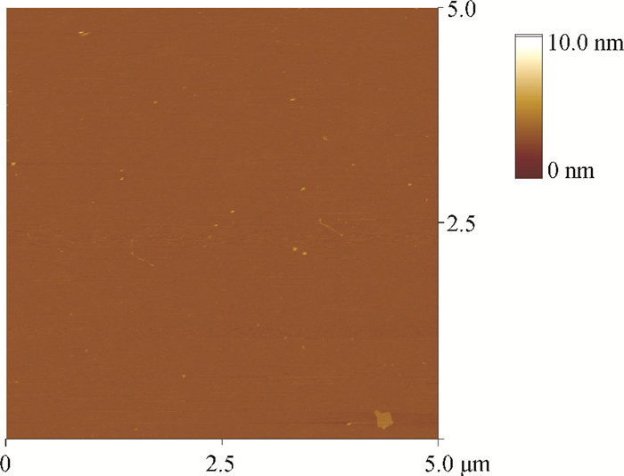
Fig. 1.
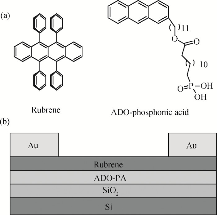
(a) Chemical structure of the rubrene and ADO-PA SAMs. (b) Device structure of the thin-film transistors
SEMICONDUCTOR DEVICES
Zhefeng Li and Xianye Luo
Corresponding author: Li Zhefeng, Email:zhefeng@cqu.edu.cn
Abstract: This study explores a strategy of using the phosphonic acid derivative (11-((12-(anthracen-2-yl)dodecyl)oxy)-11-oxoundecyl) phosphonic acid (ADO-phosphonic acid) as self-assembled monolayers (SAMs) on a Si/SiO2 surface to induce the crystallization of rubrene in vacuum deposited thin film transistors, which showed a field-effect mobility as high as 0.18 cm2/(V·s). It is found that ADO-phosphonic acid SAMs play a unique role in modulating the morphology of rubrene to form a crystalline film in the thin-film transistors.
Keywords: thin film transistors, self-assembled monolayer, phosphonic acid derivative
| [1] |
Tang M L, Reichardt A D, Wei P, et al. Correlating carrier type with frontier molecular orbital energy levels in organic thin film transistors of functionalized acene derivatives. J Am Chem Soc, 2009, 131:5264 doi: 10.1021/ja809659b
|
| [2] |
Dodabalapur A. Semiconductor technology-negatively successful. Nature, 2005, 434:151 http://adsabs.harvard.edu/abs/2005Natur.434..151D
|
| [3] |
Sirringhaus H. Device physics of Solution-processed organic field-effect transistors. Adv Mater, 2005, 17:2411 doi: 10.1002/(ISSN)1521-4095
|
| [4] |
Roberts M E, LeMieux M C, Bao Z N. Sorted and aligned single-walled carbon nanotube networks for transistor-based aqueous chemical sensors. ACS Nano, 2009, 10:3287 doi: 10.1021/nn900808b?src=recsys&journalCode=ancac3
|
| [5] |
Li Z F, Du J, Tang Q, et al. Induced crystallization of rubrene in thin-film transistors. Adv Mater, 2010, 22:3242 doi: 10.1002/adma.201000786
|
| [6] |
Hwang S K, Bae I, Cho S M, et al. High performance multi-level non-volatile polymer memory with solution-blended ferroelectric polymer/high-k insulators for low voltage operation. Adv Funct Mater, 2013, 23:5484 doi: 10.1002/adfm.v23.44
|
| [7] |
Tsai T D, Chang J W, Wen T C, et al. Manipulating the hysteresis in poly(vinyl alcohol)-dielectric organic field-effect transistors toward memory elements. Adv Funct Mater, 2013, 23:4206 doi: 10.1002/adfm.v23.34
|
| [8] |
Majewski L A, Schroeder R, Grell M. One volt organic transistor. Adv Mater, 2005, 17:192 doi: 10.1002/(ISSN)1521-4095
|
| [9] |
Zirkl M, Haase A, Fian A, et al. Low-voltage organic thin-film transistors with high-k nanocomposite gate dielectrics for flexible electronics and optothermal sensors. Adv Mater, 2007, 19:2241 doi: 10.1002/(ISSN)1521-4095
|
| [10] |
Lee B H, Ryu M K, Choi S Y, et al. Rapid vapor-phase fabrication of organic-inorganic hybrid superlattices with monolayer precision. J Am Chem Soc, 2007, 129:16034 doi: 10.1021/ja075664o
|
| [11] |
Park B, Cho S E, Kim Y, et al. Simultaneous study of exciton diffusion/dissociation and charge transport in a donor-acceptor bilayer:pentacene on a C60-terminated self-assembled monolayer. Adv Mater, 2013, 25:6453 doi: 10.1002/adma.v25.44
|
| [12] |
Ulman A. Formation and structure of self-assembled monolayers. Chem Rev, 1996, 96:1533 doi: 10.1021/cr9502357
|
| [13] |
Onclin S, Ravoo B J, Reinhoudt D N. Engineering silicon oxide surfaces using self-assembled monolayers. Angew Chem Int. Ed, 2005, 44:6282 doi: 10.1002/(ISSN)1521-3773
|
| [14] |
Walter S R, Youn J, Emery J D, et al. In-situ probe of gate dielectric-semiconductor interfacial order in organic transistors:origin and control of large performance sensitivities. J Am Chem Soc, 2012, 134(28):11726 doi: 10.1021/ja3036493
|
| [15] |
Halik M, Hirsch A. The potential of molecular self-assembled monolayers in organic electronic devices. Adv Mater, 2011, 23:2689 doi: 10.1002/adma.v23.22/23
|
| [16] |
Silverman B M, Wieghaus K A, Schwartz J. Comparative properties of siloxane vs phosphonate monolayers on a key titanium alloy. Langmuir, 2005, 21:225 doi: 10.1021/la048227l
|
| [17] |
Liakos I L, McAlpine E, Chen X Y, et al. Assembly of octadecyl phosphonic acid on the α-Al2O3 (0001) surface of air annealed alumina:evidence for termination dependent adsorption. Appl Surf Sci, 2008, 255(5):3276 doi: 10.1016/j.apsusc.2008.09.037
|
| [18] |
Hanson E L, Schwartz J, Nickel B, et al. Bonding self-assembled, compact organophosphonate monolayers to the native oxide surface of silicon. J Am Chem Soc, 2003, 125(51):16074 doi: 10.1021/ja035956z
|
| [19] |
Guo X, Qin C J, Cheng Y X, et al. White electroluminescence from a phosphonate-functionalized single-polymer system with electron-trapping effect. Adv Mater, 2009, 21:3682 doi: 10.1002/adma.v21:36
|
| [20] |
Kang M S, Ma H, Yip H L, et al. Direct surface functionalization of indium tin oxide via electrochemically induced assembly. J Mater Chem, 2007, 17:3489 doi: 10.1039/b705559e
|
| [21] |
Klauk H, Zschieschang U, Pflaum J, et al. Ultralow-power organic complementary circuits. Nature, 2007, 445:745 doi: 10.1038/nature05533
|
| [22] |
Jurchescu O D, Meetsma A, Palstra T T M. Low-temperature structure of rubrene single crystals grown by vapor transport. Acta Crystallographica Section B:Structural Science, 2006, 62:330 doi: 10.1107/S0108768106003053
|
| [23] |
Yang S Y, Shin K, Park C E. The effect of gate-dielectric surface energy on pentacene morphology and organic field-effect transistor characteristics. Adv Funct Mater, 2005, 15:1806 doi: 10.1002/(ISSN)1616-3028
|

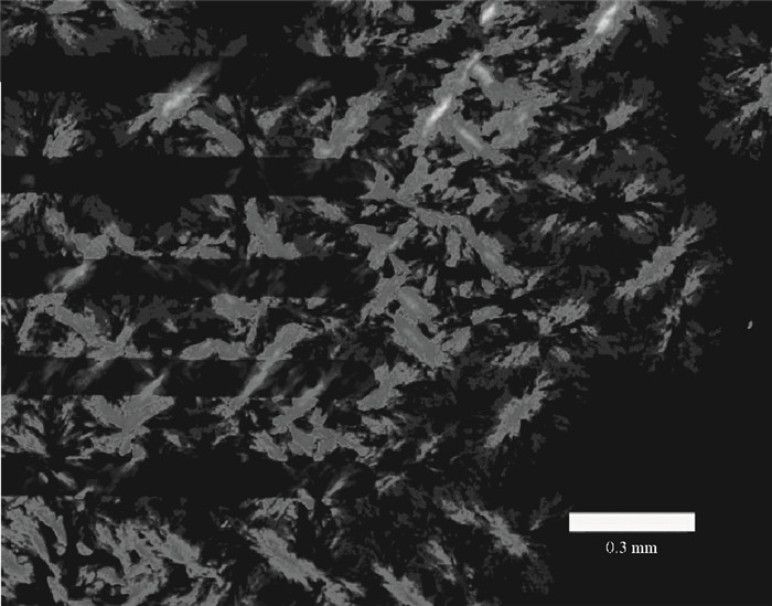
Table 1. Device characteristics of rubrene on different dielectric surfaces.

|
| [1] |
Tang M L, Reichardt A D, Wei P, et al. Correlating carrier type with frontier molecular orbital energy levels in organic thin film transistors of functionalized acene derivatives. J Am Chem Soc, 2009, 131:5264 doi: 10.1021/ja809659b
|
| [2] |
Dodabalapur A. Semiconductor technology-negatively successful. Nature, 2005, 434:151 http://adsabs.harvard.edu/abs/2005Natur.434..151D
|
| [3] |
Sirringhaus H. Device physics of Solution-processed organic field-effect transistors. Adv Mater, 2005, 17:2411 doi: 10.1002/(ISSN)1521-4095
|
| [4] |
Roberts M E, LeMieux M C, Bao Z N. Sorted and aligned single-walled carbon nanotube networks for transistor-based aqueous chemical sensors. ACS Nano, 2009, 10:3287 doi: 10.1021/nn900808b?src=recsys&journalCode=ancac3
|
| [5] |
Li Z F, Du J, Tang Q, et al. Induced crystallization of rubrene in thin-film transistors. Adv Mater, 2010, 22:3242 doi: 10.1002/adma.201000786
|
| [6] |
Hwang S K, Bae I, Cho S M, et al. High performance multi-level non-volatile polymer memory with solution-blended ferroelectric polymer/high-k insulators for low voltage operation. Adv Funct Mater, 2013, 23:5484 doi: 10.1002/adfm.v23.44
|
| [7] |
Tsai T D, Chang J W, Wen T C, et al. Manipulating the hysteresis in poly(vinyl alcohol)-dielectric organic field-effect transistors toward memory elements. Adv Funct Mater, 2013, 23:4206 doi: 10.1002/adfm.v23.34
|
| [8] |
Majewski L A, Schroeder R, Grell M. One volt organic transistor. Adv Mater, 2005, 17:192 doi: 10.1002/(ISSN)1521-4095
|
| [9] |
Zirkl M, Haase A, Fian A, et al. Low-voltage organic thin-film transistors with high-k nanocomposite gate dielectrics for flexible electronics and optothermal sensors. Adv Mater, 2007, 19:2241 doi: 10.1002/(ISSN)1521-4095
|
| [10] |
Lee B H, Ryu M K, Choi S Y, et al. Rapid vapor-phase fabrication of organic-inorganic hybrid superlattices with monolayer precision. J Am Chem Soc, 2007, 129:16034 doi: 10.1021/ja075664o
|
| [11] |
Park B, Cho S E, Kim Y, et al. Simultaneous study of exciton diffusion/dissociation and charge transport in a donor-acceptor bilayer:pentacene on a C60-terminated self-assembled monolayer. Adv Mater, 2013, 25:6453 doi: 10.1002/adma.v25.44
|
| [12] |
Ulman A. Formation and structure of self-assembled monolayers. Chem Rev, 1996, 96:1533 doi: 10.1021/cr9502357
|
| [13] |
Onclin S, Ravoo B J, Reinhoudt D N. Engineering silicon oxide surfaces using self-assembled monolayers. Angew Chem Int. Ed, 2005, 44:6282 doi: 10.1002/(ISSN)1521-3773
|
| [14] |
Walter S R, Youn J, Emery J D, et al. In-situ probe of gate dielectric-semiconductor interfacial order in organic transistors:origin and control of large performance sensitivities. J Am Chem Soc, 2012, 134(28):11726 doi: 10.1021/ja3036493
|
| [15] |
Halik M, Hirsch A. The potential of molecular self-assembled monolayers in organic electronic devices. Adv Mater, 2011, 23:2689 doi: 10.1002/adma.v23.22/23
|
| [16] |
Silverman B M, Wieghaus K A, Schwartz J. Comparative properties of siloxane vs phosphonate monolayers on a key titanium alloy. Langmuir, 2005, 21:225 doi: 10.1021/la048227l
|
| [17] |
Liakos I L, McAlpine E, Chen X Y, et al. Assembly of octadecyl phosphonic acid on the α-Al2O3 (0001) surface of air annealed alumina:evidence for termination dependent adsorption. Appl Surf Sci, 2008, 255(5):3276 doi: 10.1016/j.apsusc.2008.09.037
|
| [18] |
Hanson E L, Schwartz J, Nickel B, et al. Bonding self-assembled, compact organophosphonate monolayers to the native oxide surface of silicon. J Am Chem Soc, 2003, 125(51):16074 doi: 10.1021/ja035956z
|
| [19] |
Guo X, Qin C J, Cheng Y X, et al. White electroluminescence from a phosphonate-functionalized single-polymer system with electron-trapping effect. Adv Mater, 2009, 21:3682 doi: 10.1002/adma.v21:36
|
| [20] |
Kang M S, Ma H, Yip H L, et al. Direct surface functionalization of indium tin oxide via electrochemically induced assembly. J Mater Chem, 2007, 17:3489 doi: 10.1039/b705559e
|
| [21] |
Klauk H, Zschieschang U, Pflaum J, et al. Ultralow-power organic complementary circuits. Nature, 2007, 445:745 doi: 10.1038/nature05533
|
| [22] |
Jurchescu O D, Meetsma A, Palstra T T M. Low-temperature structure of rubrene single crystals grown by vapor transport. Acta Crystallographica Section B:Structural Science, 2006, 62:330 doi: 10.1107/S0108768106003053
|
| [23] |
Yang S Y, Shin K, Park C E. The effect of gate-dielectric surface energy on pentacene morphology and organic field-effect transistor characteristics. Adv Funct Mater, 2005, 15:1806 doi: 10.1002/(ISSN)1616-3028
|


Article views: 2714 Times PDF downloads: 18 Times Cited by: 0 Times
Received: 26 March 2014 Revised: 14 May 2014 Online: Published: 01 October 2014
| Citation: |
Zhefeng Li, Xianye Luo. ADO-phosphonic acid self-assembled monolayer modified dielectrics for organic thin film transistors[J]. Journal of Semiconductors, 2014, 35(10): 104004. doi: 10.1088/1674-4926/35/10/104004
****
Z F Li, X Y Luo. ADO-phosphonic acid self-assembled monolayer modified dielectrics for organic thin film transistors[J]. J. Semicond., 2014, 35(10): 104004. doi: 10.1088/1674-4926/35/10/104004.

|
| [1] |
Tang M L, Reichardt A D, Wei P, et al. Correlating carrier type with frontier molecular orbital energy levels in organic thin film transistors of functionalized acene derivatives. J Am Chem Soc, 2009, 131:5264 doi: 10.1021/ja809659b
|
| [2] |
Dodabalapur A. Semiconductor technology-negatively successful. Nature, 2005, 434:151 http://adsabs.harvard.edu/abs/2005Natur.434..151D
|
| [3] |
Sirringhaus H. Device physics of Solution-processed organic field-effect transistors. Adv Mater, 2005, 17:2411 doi: 10.1002/(ISSN)1521-4095
|
| [4] |
Roberts M E, LeMieux M C, Bao Z N. Sorted and aligned single-walled carbon nanotube networks for transistor-based aqueous chemical sensors. ACS Nano, 2009, 10:3287 doi: 10.1021/nn900808b?src=recsys&journalCode=ancac3
|
| [5] |
Li Z F, Du J, Tang Q, et al. Induced crystallization of rubrene in thin-film transistors. Adv Mater, 2010, 22:3242 doi: 10.1002/adma.201000786
|
| [6] |
Hwang S K, Bae I, Cho S M, et al. High performance multi-level non-volatile polymer memory with solution-blended ferroelectric polymer/high-k insulators for low voltage operation. Adv Funct Mater, 2013, 23:5484 doi: 10.1002/adfm.v23.44
|
| [7] |
Tsai T D, Chang J W, Wen T C, et al. Manipulating the hysteresis in poly(vinyl alcohol)-dielectric organic field-effect transistors toward memory elements. Adv Funct Mater, 2013, 23:4206 doi: 10.1002/adfm.v23.34
|
| [8] |
Majewski L A, Schroeder R, Grell M. One volt organic transistor. Adv Mater, 2005, 17:192 doi: 10.1002/(ISSN)1521-4095
|
| [9] |
Zirkl M, Haase A, Fian A, et al. Low-voltage organic thin-film transistors with high-k nanocomposite gate dielectrics for flexible electronics and optothermal sensors. Adv Mater, 2007, 19:2241 doi: 10.1002/(ISSN)1521-4095
|
| [10] |
Lee B H, Ryu M K, Choi S Y, et al. Rapid vapor-phase fabrication of organic-inorganic hybrid superlattices with monolayer precision. J Am Chem Soc, 2007, 129:16034 doi: 10.1021/ja075664o
|
| [11] |
Park B, Cho S E, Kim Y, et al. Simultaneous study of exciton diffusion/dissociation and charge transport in a donor-acceptor bilayer:pentacene on a C60-terminated self-assembled monolayer. Adv Mater, 2013, 25:6453 doi: 10.1002/adma.v25.44
|
| [12] |
Ulman A. Formation and structure of self-assembled monolayers. Chem Rev, 1996, 96:1533 doi: 10.1021/cr9502357
|
| [13] |
Onclin S, Ravoo B J, Reinhoudt D N. Engineering silicon oxide surfaces using self-assembled monolayers. Angew Chem Int. Ed, 2005, 44:6282 doi: 10.1002/(ISSN)1521-3773
|
| [14] |
Walter S R, Youn J, Emery J D, et al. In-situ probe of gate dielectric-semiconductor interfacial order in organic transistors:origin and control of large performance sensitivities. J Am Chem Soc, 2012, 134(28):11726 doi: 10.1021/ja3036493
|
| [15] |
Halik M, Hirsch A. The potential of molecular self-assembled monolayers in organic electronic devices. Adv Mater, 2011, 23:2689 doi: 10.1002/adma.v23.22/23
|
| [16] |
Silverman B M, Wieghaus K A, Schwartz J. Comparative properties of siloxane vs phosphonate monolayers on a key titanium alloy. Langmuir, 2005, 21:225 doi: 10.1021/la048227l
|
| [17] |
Liakos I L, McAlpine E, Chen X Y, et al. Assembly of octadecyl phosphonic acid on the α-Al2O3 (0001) surface of air annealed alumina:evidence for termination dependent adsorption. Appl Surf Sci, 2008, 255(5):3276 doi: 10.1016/j.apsusc.2008.09.037
|
| [18] |
Hanson E L, Schwartz J, Nickel B, et al. Bonding self-assembled, compact organophosphonate monolayers to the native oxide surface of silicon. J Am Chem Soc, 2003, 125(51):16074 doi: 10.1021/ja035956z
|
| [19] |
Guo X, Qin C J, Cheng Y X, et al. White electroluminescence from a phosphonate-functionalized single-polymer system with electron-trapping effect. Adv Mater, 2009, 21:3682 doi: 10.1002/adma.v21:36
|
| [20] |
Kang M S, Ma H, Yip H L, et al. Direct surface functionalization of indium tin oxide via electrochemically induced assembly. J Mater Chem, 2007, 17:3489 doi: 10.1039/b705559e
|
| [21] |
Klauk H, Zschieschang U, Pflaum J, et al. Ultralow-power organic complementary circuits. Nature, 2007, 445:745 doi: 10.1038/nature05533
|
| [22] |
Jurchescu O D, Meetsma A, Palstra T T M. Low-temperature structure of rubrene single crystals grown by vapor transport. Acta Crystallographica Section B:Structural Science, 2006, 62:330 doi: 10.1107/S0108768106003053
|
| [23] |
Yang S Y, Shin K, Park C E. The effect of gate-dielectric surface energy on pentacene morphology and organic field-effect transistor characteristics. Adv Funct Mater, 2005, 15:1806 doi: 10.1002/(ISSN)1616-3028
|

 WeChat ID
Journal of Semiconductors © 2017 All Rights Reserved 京ICP备05085259号-2

 DownLoad: