Citation: |
Hengliang Zhao, Huilong Zhu, Jian Zhong, Xiaolong Ma, Xing Wei, Chao Zhao, Dapeng Chen, Tianchun Ye. Simulations of backgate sandwich nanowire MOSFETs with improved device performance[J]. Journal of Semiconductors, 2014, 35(10): 104005. doi: 10.1088/1674-4926/35/10/104005
****
H L Zhao, H L Zhu, J Zhong, X L Ma, X Wei, C Zhao, D P Chen, T C Ye. Simulations of backgate sandwich nanowire MOSFETs with improved device performance[J]. J. Semicond., 2014, 35(10): 104005. doi: 10.1088/1674-4926/35/10/104005.
|
Simulations of backgate sandwich nanowire MOSFETs with improved device performance
DOI: 10.1088/1674-4926/35/10/104005
More Information
-
Abstract
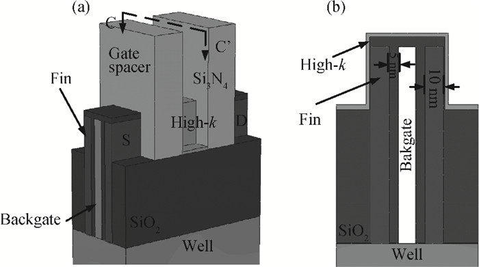
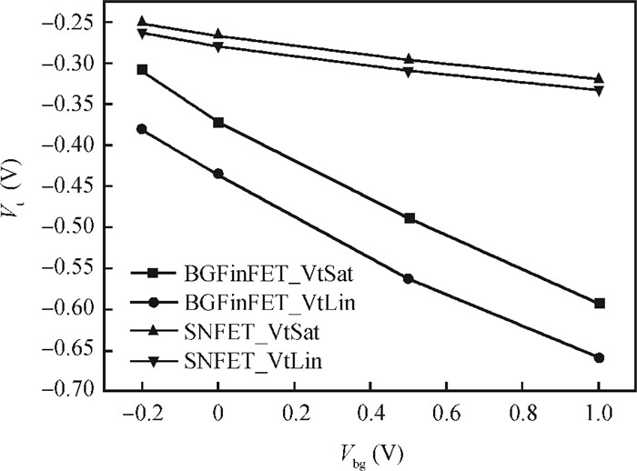
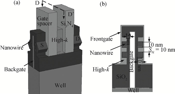
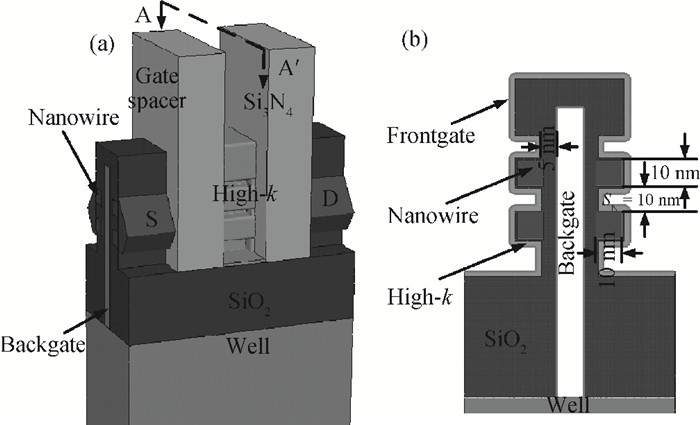
We propose a novel backgate sandwich nanowire MOSFET (SNFET), which offers the advantages of ETSOI (dynamic backgate voltage controllability) and nanowire FETs (good short channel effect). A backgate is used for threshold voltage (Vt) control of the SNFET. Compared with a backgate FinFET with a punch-through stop layer (PTSL), the SNFET possesses improved device performance. 3D device simulations indicate that the SNFET has a three times larger overdrive current, a~75% smaller off leakage current, and reduced subthreshold swing (SS) and DIBL than those of a backgate FinFET when the nanowire (NW) and the fin are of equal width. A new process flow to fabricate the backgate SNFET is also proposed in this work. Our analytical model suggests that Vt control by the backgate can be attributed to the capacitances formed by the frontgate, NW, and backgate. The SNFET devices are compatible with the latest state-of-the-art high-k/metal gate CMOS technology with the unique capability of independent backgate control for nFETs and pFETs, which is promising for sub-22 nm scaling down.-
Keywords:
- sandwich nanowire MOSFET,
- backgate,
- TCAD,
- analytical model
-
References
[1] Shrivastava M, Verma B, Baghini M S, et al. Benchmarking the device performance at sub 22 nm node technologies using an SoC framework. IEEE International Electron Devices Meeting (IEDM), 2009:1[2] De Marchi M, Sacchetto D, Frache S, et al. Polarity control in double-gate, gate-all-around vertically stacked silicon nanowire FETs. IEEE International Electron Devices Meeting (IEDM), 2012:8.4.1[3] Wu C C, Lin D W, Keshavarzi A, et al. High performance 22/20 nm FinFET CMOS devices with advanced high-K/metal gate scheme. IEEE International Electron Devices Meeting (IEDM), 2010:27.1.1[4] Sinha S, Chaudhury S. Impact of oxide thickness on gate capacitance-a comprehensive analysis on MOSFET. Nanowire FET and CNTFET Devices, 2013[5] Khakifirooz A, Cheng K, Reznicek A, et al. Scalability of extremely thin SOI (ETSOI) MOSFETs to sub-20-nm gate length. IEEE Electron Device Lett, 2012, 33(2):149 doi: 10.1109/LED.2011.2174411[6] Kuhn K J. CMOS transistor scaling past 32 nm and implications on variation. IEEE Journal of Advanced Semiconductor Manufacturing Conference (ASMC), 2010:241[7] Yau J B, Cai J, Shi L, et al. FDSOI CMOS with dual backgate control for performance and power modulation. IEEE International Symposium on VLSI Technology, Systems, and Applications, 2009:84[8] Sugii N, Tsuchiya R, Ishigaki T, et al. Local Vth variability and scalability in silicon-on-thin-BOX (SOTB) CMOS with small random-dopant fluctuation. IEEE Trans Electron Devices, 2010, 57(4):835 doi: 10.1109/TED.2010.2040664[9] Yamaoka M, Tsuchiya R, Kawahara T. SRAM circuit with expanded operating margin and reduced stand-by leakage current using thin-BOX FD-SOI transistors. IEEE J Solid-State Circuits, 2006, 41(11):2366 doi: 10.1109/JSSC.2006.882891[10] TCAD Sentaurus User Manual. Synopsys Inc, 2010. 12[11] Xu M, Zhu H, Wu H, et al. Simulations of bulk FinFETs with body gate controlling punch through leakage. ECS Transactions, 2013, 52(1):67 doi: 10.1149/05201.0067ecst[12] Tomida K, Popovici M, Opsomer K, et al. Non-linear dielectric constant increase with Ti composition in high-k ALD-HfTiOx films after O2 crystallization annealing. IOP Conference Series:Materials Science and Engineering, IOP Publishing, 2010, 8(1):012023[13] FinFETs and other multi-gate transistors. Springer, 2008: 82[14] Coquand R, Barraud S, Cassé M, et al. Scaling of high-k/metal-gate trigate SOI nanowire transistors down to 10 nm width. IEEE 13th International Conference on Ultimate Integration on Silicon (ULIS), 2012:37 -
Proportional views