Fig. 1.
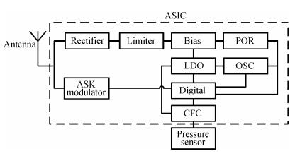
System design
SEMICONDUCTOR INTEGRATED CIRCUITS
Demeng Liu1, 2, Niansong Mei1, 2 and Zhaofeng Zhang1, 2,
Corresponding author: Zhang Zhaofeng, Email:zhangzf@sari.ac.cn
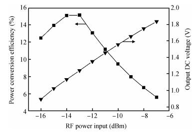
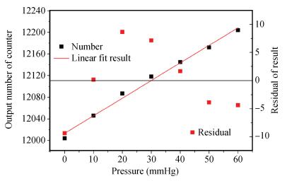
Abstract: This paper describes an ultralow power wireless intraocular pressure (IOP) monitoring system that is dedicated to sensing and transferring intraocular pressure of glaucoma patients. Our system is comprised of a capacitive pressure sensor, an application-specific integrated circuit, which is designed on the SMIC 180 nm process, and a dipole antenna. The system is wirelessly powered and demonstrates a power consumption of 7.56 μW at 1.24 V during continuous monitoring, a significant reduction in active power dissipation compared to existing work. The input RF sensitivity is -13 dBm. A significant reduction in input RF sensitivity results from the reduction of mismatch time of the ASK modulation caused by FM0 encoding. The system exhibits an average error of ±1.5 mmHg in measured pressure. Finally, a complete IOP system is demonstrated in the real biological environment, showing a successful reading of the pressure of an eye.
Keywords: IOP, implanted medical, pressure measurement, RF powering, ultralow power ASIC
| [1] |
Quigley H, Broman A. The number of people with glaucoma worldwide in 2010 and 2020. British Journal of Ophthalmology, 2006, 90(3):262 doi: 10.1136/bjo.2005.081224
|
| [2] |
Katuri K C, Asrani S, Ramasubramanian M K. Intraocular pressure monitoring sensors. IEEE Sensors Journal, 2008, 8(1):12
|
| [3] |
Shih Y C, Shen T, Otis B. A 2.3μW wireless intraocular pressure/temperature monitor. IEEE J Solid-State Circuits, 2011, 46(11):1 doi: 10.1109/JSSC.2011.2172727
|
| [4] |
Chen G, Ghaed H, Haque R, et al. A cubic-millimeter energy-autonomous wireless intraocular pressure monitor. IEEE International Solid-State Circuits Conference Digest of Technical Papers (ISSCC), San Francisco, USA, 2011:310
|
| [5] |
Chow E Y, Chlebowski A L, Irazoqui P P. A miniature-implantable RF-wireless active glaucoma intraocular pressure monitor. IEEE Trans Biomedical Circuits Syst, 2010, 4(6):340 doi: 10.1109/TBCAS.2010.2081364
|
| [6] |
Chen P J, Saati S, Varma R, et al. Wireless intraocular pressure sensing using microfabricated minimally invasive flexible-coiled LC sensor implant. J Microelectromechan Syst, 2010, 19(4):721 doi: 10.1109/JMEMS.2010.2049825
|
| [7] |
Leonardi M, Pitchon E M, Bertsch A, et al. Wireless contact lens sensor for intraocular pressure monitoring:assessment on enucleated pig eyes. Acta Ophthalmologica, 2009, 87(4):433 doi: 10.1111/aos.2009.87.issue-4
|
| [8] |
Liu Demeng, Wu Miao, Mei Niansong, et al. Development and outlook of wireless implantable continuously intraocular pressure detection microsystem. Micronanoelectron Technol, 2013, 50(1):57
|
| [9] |
Capacitive Pressure Sensor E1. 3N, M. Bremen, Editor 2008: Bremen
|
| [10] |
Kim S, Scholz O. Implantable active telemetry system using microcoils. Conf Proc IEEE Eng Med Biol Soc, 2005, 7:7147
|
| [11] |
Stangel K, Kolnsberg S, Hammerschmidt D, et al. A programmable intraocular CMOS pressure sensor system implant. IEEE J Solid-State Circuits, 2001, 36(7):1094 doi: 10.1109/4.933466
|
| [12] |
Gemio J, Parron J, Soler J. Human body effects on implantable antennas for ISM bands applications:models comparison and propagation losses study. Progress in Electromagnetics Research, 2010, 110:437 doi: 10.2528/PIER10102604
|
| [13] |
Poon A S Y, O'Driscoll S, Meng T H. Optimal operating frequency in wireless power transmission for implantable devices. 29th Annual International Conference of the IEEE Engineering in Medicine and Biology Society, 2007:5673
|
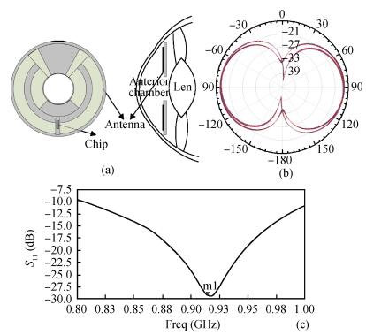
Table 1. Power dissipation of main modules

|
Table 2. IOP monitoring system comparison

|
| [1] |
Quigley H, Broman A. The number of people with glaucoma worldwide in 2010 and 2020. British Journal of Ophthalmology, 2006, 90(3):262 doi: 10.1136/bjo.2005.081224
|
| [2] |
Katuri K C, Asrani S, Ramasubramanian M K. Intraocular pressure monitoring sensors. IEEE Sensors Journal, 2008, 8(1):12
|
| [3] |
Shih Y C, Shen T, Otis B. A 2.3μW wireless intraocular pressure/temperature monitor. IEEE J Solid-State Circuits, 2011, 46(11):1 doi: 10.1109/JSSC.2011.2172727
|
| [4] |
Chen G, Ghaed H, Haque R, et al. A cubic-millimeter energy-autonomous wireless intraocular pressure monitor. IEEE International Solid-State Circuits Conference Digest of Technical Papers (ISSCC), San Francisco, USA, 2011:310
|
| [5] |
Chow E Y, Chlebowski A L, Irazoqui P P. A miniature-implantable RF-wireless active glaucoma intraocular pressure monitor. IEEE Trans Biomedical Circuits Syst, 2010, 4(6):340 doi: 10.1109/TBCAS.2010.2081364
|
| [6] |
Chen P J, Saati S, Varma R, et al. Wireless intraocular pressure sensing using microfabricated minimally invasive flexible-coiled LC sensor implant. J Microelectromechan Syst, 2010, 19(4):721 doi: 10.1109/JMEMS.2010.2049825
|
| [7] |
Leonardi M, Pitchon E M, Bertsch A, et al. Wireless contact lens sensor for intraocular pressure monitoring:assessment on enucleated pig eyes. Acta Ophthalmologica, 2009, 87(4):433 doi: 10.1111/aos.2009.87.issue-4
|
| [8] |
Liu Demeng, Wu Miao, Mei Niansong, et al. Development and outlook of wireless implantable continuously intraocular pressure detection microsystem. Micronanoelectron Technol, 2013, 50(1):57
|
| [9] |
Capacitive Pressure Sensor E1. 3N, M. Bremen, Editor 2008: Bremen
|
| [10] |
Kim S, Scholz O. Implantable active telemetry system using microcoils. Conf Proc IEEE Eng Med Biol Soc, 2005, 7:7147
|
| [11] |
Stangel K, Kolnsberg S, Hammerschmidt D, et al. A programmable intraocular CMOS pressure sensor system implant. IEEE J Solid-State Circuits, 2001, 36(7):1094 doi: 10.1109/4.933466
|
| [12] |
Gemio J, Parron J, Soler J. Human body effects on implantable antennas for ISM bands applications:models comparison and propagation losses study. Progress in Electromagnetics Research, 2010, 110:437 doi: 10.2528/PIER10102604
|
| [13] |
Poon A S Y, O'Driscoll S, Meng T H. Optimal operating frequency in wireless power transmission for implantable devices. 29th Annual International Conference of the IEEE Engineering in Medicine and Biology Society, 2007:5673
|


Article views: 2901 Times PDF downloads: 11 Times Cited by: 0 Times
Received: 05 March 2014 Revised: 23 April 2014 Online: Published: 01 October 2014
| Citation: |
Demeng Liu, Niansong Mei, Zhaofeng Zhang. An ultralow power wireless intraocular pressure monitoring system[J]. Journal of Semiconductors, 2014, 35(10): 105014. doi: 10.1088/1674-4926/35/10/105014
****
D M Liu, N S Mei, Z F Zhang. An ultralow power wireless intraocular pressure monitoring system[J]. J. Semicond., 2014, 35(10): 105014. doi: 10.1088/1674-4926/35/10/105014.

|
| [1] |
Quigley H, Broman A. The number of people with glaucoma worldwide in 2010 and 2020. British Journal of Ophthalmology, 2006, 90(3):262 doi: 10.1136/bjo.2005.081224
|
| [2] |
Katuri K C, Asrani S, Ramasubramanian M K. Intraocular pressure monitoring sensors. IEEE Sensors Journal, 2008, 8(1):12
|
| [3] |
Shih Y C, Shen T, Otis B. A 2.3μW wireless intraocular pressure/temperature monitor. IEEE J Solid-State Circuits, 2011, 46(11):1 doi: 10.1109/JSSC.2011.2172727
|
| [4] |
Chen G, Ghaed H, Haque R, et al. A cubic-millimeter energy-autonomous wireless intraocular pressure monitor. IEEE International Solid-State Circuits Conference Digest of Technical Papers (ISSCC), San Francisco, USA, 2011:310
|
| [5] |
Chow E Y, Chlebowski A L, Irazoqui P P. A miniature-implantable RF-wireless active glaucoma intraocular pressure monitor. IEEE Trans Biomedical Circuits Syst, 2010, 4(6):340 doi: 10.1109/TBCAS.2010.2081364
|
| [6] |
Chen P J, Saati S, Varma R, et al. Wireless intraocular pressure sensing using microfabricated minimally invasive flexible-coiled LC sensor implant. J Microelectromechan Syst, 2010, 19(4):721 doi: 10.1109/JMEMS.2010.2049825
|
| [7] |
Leonardi M, Pitchon E M, Bertsch A, et al. Wireless contact lens sensor for intraocular pressure monitoring:assessment on enucleated pig eyes. Acta Ophthalmologica, 2009, 87(4):433 doi: 10.1111/aos.2009.87.issue-4
|
| [8] |
Liu Demeng, Wu Miao, Mei Niansong, et al. Development and outlook of wireless implantable continuously intraocular pressure detection microsystem. Micronanoelectron Technol, 2013, 50(1):57
|
| [9] |
Capacitive Pressure Sensor E1. 3N, M. Bremen, Editor 2008: Bremen
|
| [10] |
Kim S, Scholz O. Implantable active telemetry system using microcoils. Conf Proc IEEE Eng Med Biol Soc, 2005, 7:7147
|
| [11] |
Stangel K, Kolnsberg S, Hammerschmidt D, et al. A programmable intraocular CMOS pressure sensor system implant. IEEE J Solid-State Circuits, 2001, 36(7):1094 doi: 10.1109/4.933466
|
| [12] |
Gemio J, Parron J, Soler J. Human body effects on implantable antennas for ISM bands applications:models comparison and propagation losses study. Progress in Electromagnetics Research, 2010, 110:437 doi: 10.2528/PIER10102604
|
| [13] |
Poon A S Y, O'Driscoll S, Meng T H. Optimal operating frequency in wireless power transmission for implantable devices. 29th Annual International Conference of the IEEE Engineering in Medicine and Biology Society, 2007:5673
|

 WeChat ID
Journal of Semiconductors © 2017 All Rights Reserved 京ICP备05085259号-2

 DownLoad: