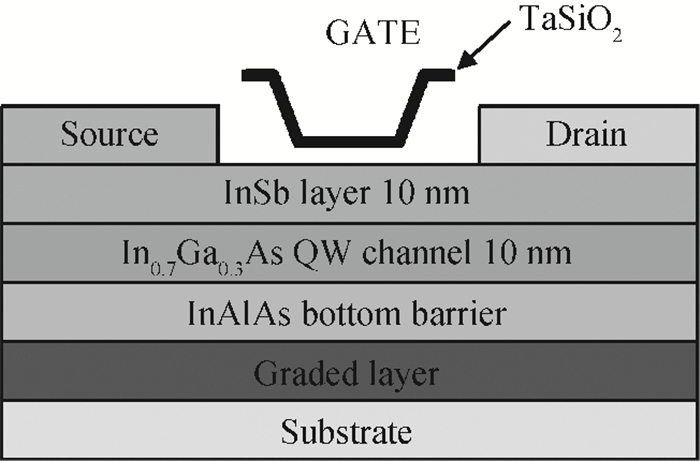
Fig. 1.
Schematic cross sectional view of HEMET.
SEMICONDUCTOR MATERIALS
T.D. Subash1, and T. Gnanasekaran2,
Corresponding author: T. D. Subash, Email:tdsubash2007@gmail.com; T. Gnanasekaran, Email:t.gnanasekaran@gmail.com
Abstract: We report on an indium antimonide high electron mobility transistor with record cut-off frequency characteristics. For high frequency response it is important to minimize parasitic resistance and capacitance to improve short-channel effects. For analog applications adequate pinch-off behavior is demonstrated. For proper device scaling we need high electron mobility and high electron density. Toward this end, the device design features and simulation are carried out by the Synopsys TCAD tool. A 30 nm InSb HEMT exhibits an excellent cut-off frequency of 586 GHz. To the knowledge of the authors, the obtained cut-off frequency is the highest ever reported in any FET on any material system.
Keywords: HEMT, InSb, gate length, cut-off frequency, short-channel effects
| [1] |
Snodgrass W, Hafez W, Harff N, et al. Pseudomorphic InSb/InGaAs heterojunction bipolar transistors (PHBTs) experimentally demonstrating fT=765 GHz at 25℃ increasing to fT=845 GHz at -55℃. IEDM Tech Dig, 2006:595 http://ieeexplore.ieee.org/xpls/abs_all.jsp?arnumber=4154272
|
| [2] |
Yeon S J, Park M H, Choi J, et al. 610 GHz InAlAs/In0.75GaAs metamorphic HEMTs with an ultra-short 15 nm gate. IEDM Tech Dig, 2007:613 http://ieeexplore.ieee.org/xpls/abs_all.jsp?arnumber=4419014
|
| [3] |
Lai R, Mei X B, Deal W R, et al. Sub 50 nm InP HEMT device with fmax greater than 1 THz. IEDM Tech Dig, 2007:609 http://ieeexplore.ieee.org/xpls/icp.jsp?arnumber=4419013
|
| [4] |
Rodwell M, Lee Q, Mensa S D, et al. Heterojunction bipolar transistors with greater than 1 THz extrapolated power-gain cut off frequencies. Proc 7th IEEE THz Conf, 1999:25 doi: 10.1088/1674-4926/35/11/113004/pdf
|
| [5] |
Yamashita Y, Endoh A, Shinohara K, et al. Pseudomorphic In0.52Al0.48As/In0.7Ga0.3As HEMTs with an ultrahigh fT of 562 GHz. IEEE Electron Device Lett, 2002, 23(10):573 doi: 10.1109/LED.2002.802667
|
| [6] |
Kim D H, del Alamo J A. Logic performance of 40 nm InAs HEMTs. IEDM Tech Dig, 2007:629 http://ieeexplore.ieee.org/xpls/icp.jsp?arnumber=4419018
|
| [7] |
Eugster C C, Broekaert T P E, del Alamo J A, et al. An InAlAs/InAs MODFET. IEEE Electron Device Lett, 1991, 12(12):707 doi: 10.1109/55.116963
|
| [8] |
Bennett B R, Magno R, Boos J B, et al. Antimonide-based compound semiconductors for electronic devices:a review. Solid-State Electron, 2005, 49(12):1875 doi: 10.1016/j.sse.2005.09.008
|
| [9] |
Chen K J, Enoki T, Maewawa K, et al. High performance InP-based enhancement-mode HEMTs using non-alloyed ohmic contacts and Pt-based buried-gate technologies. IEEE Trans Electron Devices, 1996, 43(2):252 doi: 10.1109/16.481725
|
| [10] |
Shinohara K, Yamashita Y, Endoh A, et al. Nanogate InP-HEMT technology for ultrahigh-speed performance. Proc IEEE 16th Int Conf IPRM, 2004:721 http://ieeexplore.ieee.org/xpls/abs_all.jsp?arnumber=1442827
|
| [11] |
Suemitsu T, Yokoyama H, Umeda Y, et al. High performance 0.1-μm gate enhancement-mode InAlAs/InGaAs HEMTs using two-step recessed gate technology. IEEE Trans Electron Devices, 1999, 46(6):1074 doi: 10.1109/16.766866
|
| [12] |
Shinohara K, Yamashita Y, Endoh A, et al. Ultrahigh-speed pseudomorphic In-GaAs/InAlAs HEMTs with 400-GHz cutoff frequency. IEEE Electron Device Lett, 2001, 22(11):507 doi: 10.1109/55.962645
|
| [13] |
Shinohara K, Yamashita Y, Endoh A, et al. Importance of gate-recess structure to the cutoff frequency of ultra-high-speed InGaAs/InAlAs HEMTs. Proc IEEE 14th Int Conf IPRM, 2002:451 https://www.mendeley.com/research-papers/importance-gaterecess-structure-cutoff-frequency-ultrahighspeed-ingaasinalas-hemts/
|
| [14] |
Suemitsu T, Yokoyama H, Ishii T, et al. 30-nm two-step recess gate InP-based InAlAs/InGaAs HEMTs. IEEE Trans Electron Devices, 2002, 49(10):1694 doi: 10.1109/TED.2002.803646
|
| [15] |
Wada S, Yamazaki J, Ishikawa M, et al. An 0.1-μm voidless double-deck-shaped (DDS) gate HJFET with reduced gate-fringing capacitance. IEEE Trans Electron Devices, 1999, 46(5):859 doi: 10.1109/16.760390
|
| [16] |
Abelard P, Baumard J F. The electrical conductivity of cubic stabilized zirconia. Pure & Appl Chem, 1995, 67(11):1891 http://www.degruyter.com/view/j/pac.1995.67.issue-11/pac199567111891/pac199567111891.xml?format=INT
|
| [17] |
Albertin K F, Valle M A, Pereyra I. Study of MOS capacitors with TiO2 and SiO2/TiO2 gate dielectric. Journal Integrated Circuits and Systems, 2007, 2:89 https://www.mendeley.com/research-papers/study-mos-capacitors-tio2-sio2-tio2-gate-dielectric/
|
| [18] |
Florian C, Traverso P A, Feudale M, et al. A C-band GaAs-pHEMT MMIC low phase noise VCO for space applications using a new cyclostationary nonlinear noise model. IEEE MTT-S International Microwave Symposium Digest (MTT), 2010:284 http://ieeexplore.ieee.org/document/5515080/
|
| [19] |
Srinidhi E R, Ma R, Kompa G. Application rules for accurate IMD characterization in GaN HEMTs. German Microwave Conference (GeMIC), 2008:1 http://ieeexplore.ieee.org/xpls/abs_all.jsp?arnumber=5757003
|
| [20] |
Liu H Y, Chou B Y, Hsu W C, et al. Enhanced AlGaN/GaN MOS-HEMT performance by using hydrogen peroxide oxidation technique. IEEE Trans Electron Devices, 2013, 60(1):213 doi: 10.1109/TED.2012.2227325
|
| [21] |
Sato J, Nagai Y, Hara S, et al. Analysis of performances of InSb HEMTs using quantum-corrected Monte Carlo simulation. International Conference on Indium Phosphide and Related Materials (IPRM), 2012:237 http://ieeexplore.ieee.org/document/6403367/
|
| [22] |
Florian C, Traverso P A, Filicori F. The charge-controlled nonlinear noise modeling approach for the design of MMIC GaAs-pHEMT VCOs for space applications. IEEE Trans Microw Theory Tech, 2011, 59(4):901 doi: 10.1109/TMTT.2011.2104976
|
| [23] |
Casto M J, Dooley S R. AlGaN/GaN HEMT temperature-dependent large-signal model thermal circuit extraction with verification through advanced thermal imaging. IEEE 10th Annual Wireless and Microwave Technology Conference, 2009 http://ieeexplore.ieee.org/xpls/icp.jsp?arnumber=5207307
|
| [24] |
Liu H Y, Lee C S, Hsu W C, et al. Investigations of AlGaN/AlN/GaN MOS-HEMTs on Si substrate by ozone water oxidation method. IEEE Trans Electron Devices, 2013, 60(7):2231 doi: 10.1109/TED.2013.2260753
|
| [25] |
Tang Z K, Huang S, Jiang M, et al. High-voltage (600-V) low-leakage low-current-collapse AlGaN/GaN HEMTs with AlN/SiNx passivation. IEEE Electron Device Lett, 2013, 34(3):366 doi: 10.1109/LED.2012.2236638
|


Article views: 2970 Times PDF downloads: 42 Times Cited by: 0 Times
Received: 27 May 2014 Revised: Online: Published: 01 November 2014
| Citation: |
T.D. Subash, T. Gnanasekaran. Indium antimonide based HEMT for RF applications[J]. Journal of Semiconductors, 2014, 35(11): 113004. doi: 10.1088/1674-4926/35/11/113004
****
T.D. Subash, T. Gnanasekaran. Indium antimonide based HEMT for RF applications[J]. J. Semicond., 2014, 35(11): 113004. doi: 10.1088/1674-4926/35/11/113004.

|
| [1] |
Snodgrass W, Hafez W, Harff N, et al. Pseudomorphic InSb/InGaAs heterojunction bipolar transistors (PHBTs) experimentally demonstrating fT=765 GHz at 25℃ increasing to fT=845 GHz at -55℃. IEDM Tech Dig, 2006:595 http://ieeexplore.ieee.org/xpls/abs_all.jsp?arnumber=4154272
|
| [2] |
Yeon S J, Park M H, Choi J, et al. 610 GHz InAlAs/In0.75GaAs metamorphic HEMTs with an ultra-short 15 nm gate. IEDM Tech Dig, 2007:613 http://ieeexplore.ieee.org/xpls/abs_all.jsp?arnumber=4419014
|
| [3] |
Lai R, Mei X B, Deal W R, et al. Sub 50 nm InP HEMT device with fmax greater than 1 THz. IEDM Tech Dig, 2007:609 http://ieeexplore.ieee.org/xpls/icp.jsp?arnumber=4419013
|
| [4] |
Rodwell M, Lee Q, Mensa S D, et al. Heterojunction bipolar transistors with greater than 1 THz extrapolated power-gain cut off frequencies. Proc 7th IEEE THz Conf, 1999:25 doi: 10.1088/1674-4926/35/11/113004/pdf
|
| [5] |
Yamashita Y, Endoh A, Shinohara K, et al. Pseudomorphic In0.52Al0.48As/In0.7Ga0.3As HEMTs with an ultrahigh fT of 562 GHz. IEEE Electron Device Lett, 2002, 23(10):573 doi: 10.1109/LED.2002.802667
|
| [6] |
Kim D H, del Alamo J A. Logic performance of 40 nm InAs HEMTs. IEDM Tech Dig, 2007:629 http://ieeexplore.ieee.org/xpls/icp.jsp?arnumber=4419018
|
| [7] |
Eugster C C, Broekaert T P E, del Alamo J A, et al. An InAlAs/InAs MODFET. IEEE Electron Device Lett, 1991, 12(12):707 doi: 10.1109/55.116963
|
| [8] |
Bennett B R, Magno R, Boos J B, et al. Antimonide-based compound semiconductors for electronic devices:a review. Solid-State Electron, 2005, 49(12):1875 doi: 10.1016/j.sse.2005.09.008
|
| [9] |
Chen K J, Enoki T, Maewawa K, et al. High performance InP-based enhancement-mode HEMTs using non-alloyed ohmic contacts and Pt-based buried-gate technologies. IEEE Trans Electron Devices, 1996, 43(2):252 doi: 10.1109/16.481725
|
| [10] |
Shinohara K, Yamashita Y, Endoh A, et al. Nanogate InP-HEMT technology for ultrahigh-speed performance. Proc IEEE 16th Int Conf IPRM, 2004:721 http://ieeexplore.ieee.org/xpls/abs_all.jsp?arnumber=1442827
|
| [11] |
Suemitsu T, Yokoyama H, Umeda Y, et al. High performance 0.1-μm gate enhancement-mode InAlAs/InGaAs HEMTs using two-step recessed gate technology. IEEE Trans Electron Devices, 1999, 46(6):1074 doi: 10.1109/16.766866
|
| [12] |
Shinohara K, Yamashita Y, Endoh A, et al. Ultrahigh-speed pseudomorphic In-GaAs/InAlAs HEMTs with 400-GHz cutoff frequency. IEEE Electron Device Lett, 2001, 22(11):507 doi: 10.1109/55.962645
|
| [13] |
Shinohara K, Yamashita Y, Endoh A, et al. Importance of gate-recess structure to the cutoff frequency of ultra-high-speed InGaAs/InAlAs HEMTs. Proc IEEE 14th Int Conf IPRM, 2002:451 https://www.mendeley.com/research-papers/importance-gaterecess-structure-cutoff-frequency-ultrahighspeed-ingaasinalas-hemts/
|
| [14] |
Suemitsu T, Yokoyama H, Ishii T, et al. 30-nm two-step recess gate InP-based InAlAs/InGaAs HEMTs. IEEE Trans Electron Devices, 2002, 49(10):1694 doi: 10.1109/TED.2002.803646
|
| [15] |
Wada S, Yamazaki J, Ishikawa M, et al. An 0.1-μm voidless double-deck-shaped (DDS) gate HJFET with reduced gate-fringing capacitance. IEEE Trans Electron Devices, 1999, 46(5):859 doi: 10.1109/16.760390
|
| [16] |
Abelard P, Baumard J F. The electrical conductivity of cubic stabilized zirconia. Pure & Appl Chem, 1995, 67(11):1891 http://www.degruyter.com/view/j/pac.1995.67.issue-11/pac199567111891/pac199567111891.xml?format=INT
|
| [17] |
Albertin K F, Valle M A, Pereyra I. Study of MOS capacitors with TiO2 and SiO2/TiO2 gate dielectric. Journal Integrated Circuits and Systems, 2007, 2:89 https://www.mendeley.com/research-papers/study-mos-capacitors-tio2-sio2-tio2-gate-dielectric/
|
| [18] |
Florian C, Traverso P A, Feudale M, et al. A C-band GaAs-pHEMT MMIC low phase noise VCO for space applications using a new cyclostationary nonlinear noise model. IEEE MTT-S International Microwave Symposium Digest (MTT), 2010:284 http://ieeexplore.ieee.org/document/5515080/
|
| [19] |
Srinidhi E R, Ma R, Kompa G. Application rules for accurate IMD characterization in GaN HEMTs. German Microwave Conference (GeMIC), 2008:1 http://ieeexplore.ieee.org/xpls/abs_all.jsp?arnumber=5757003
|
| [20] |
Liu H Y, Chou B Y, Hsu W C, et al. Enhanced AlGaN/GaN MOS-HEMT performance by using hydrogen peroxide oxidation technique. IEEE Trans Electron Devices, 2013, 60(1):213 doi: 10.1109/TED.2012.2227325
|
| [21] |
Sato J, Nagai Y, Hara S, et al. Analysis of performances of InSb HEMTs using quantum-corrected Monte Carlo simulation. International Conference on Indium Phosphide and Related Materials (IPRM), 2012:237 http://ieeexplore.ieee.org/document/6403367/
|
| [22] |
Florian C, Traverso P A, Filicori F. The charge-controlled nonlinear noise modeling approach for the design of MMIC GaAs-pHEMT VCOs for space applications. IEEE Trans Microw Theory Tech, 2011, 59(4):901 doi: 10.1109/TMTT.2011.2104976
|
| [23] |
Casto M J, Dooley S R. AlGaN/GaN HEMT temperature-dependent large-signal model thermal circuit extraction with verification through advanced thermal imaging. IEEE 10th Annual Wireless and Microwave Technology Conference, 2009 http://ieeexplore.ieee.org/xpls/icp.jsp?arnumber=5207307
|
| [24] |
Liu H Y, Lee C S, Hsu W C, et al. Investigations of AlGaN/AlN/GaN MOS-HEMTs on Si substrate by ozone water oxidation method. IEEE Trans Electron Devices, 2013, 60(7):2231 doi: 10.1109/TED.2013.2260753
|
| [25] |
Tang Z K, Huang S, Jiang M, et al. High-voltage (600-V) low-leakage low-current-collapse AlGaN/GaN HEMTs with AlN/SiNx passivation. IEEE Electron Device Lett, 2013, 34(3):366 doi: 10.1109/LED.2012.2236638
|

 WeChat ID
Journal of Semiconductors © 2017 All Rights Reserved 京ICP备05085259号-2

 DownLoad: