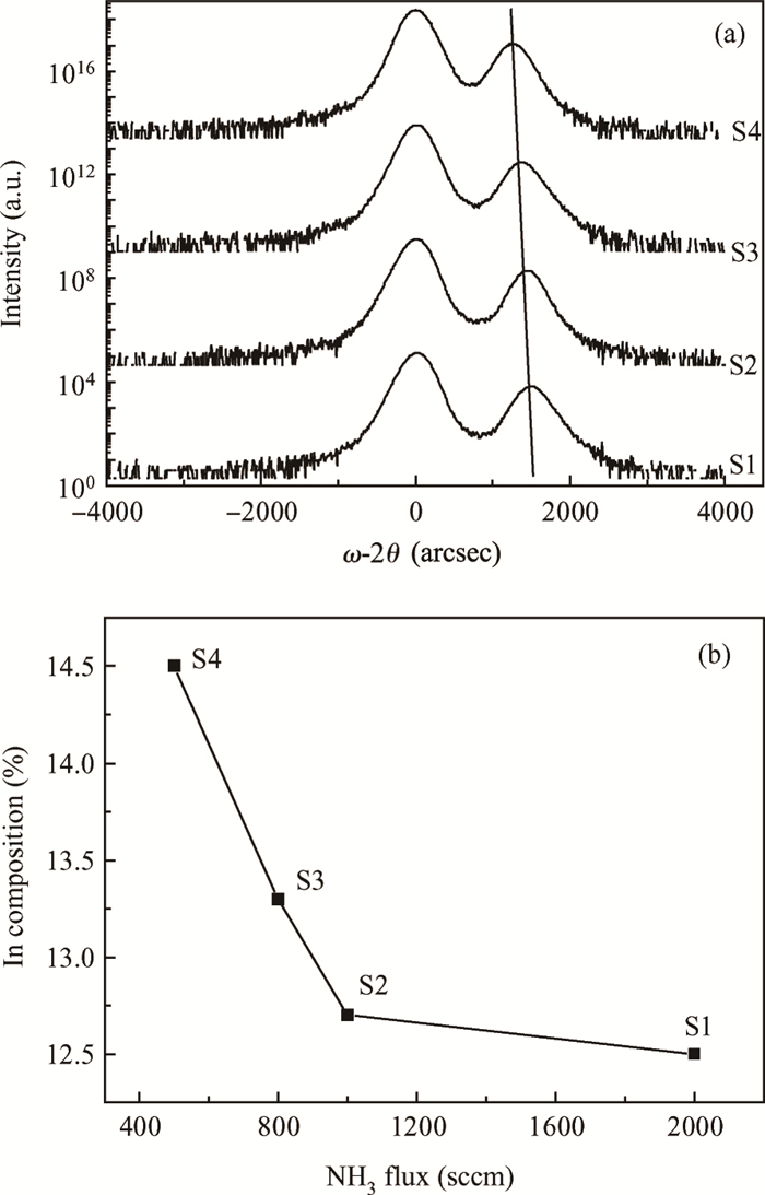
Fig. 1.
(a) XRD and (b) In composition of the samples with different NH$_{3}$ flux.
SEMICONDUCTOR MATERIALS
Bo Liu, Jiayun Yin, Yuanjie Lü, Shaobo Dun, Xiongwen Zhang, Zhihong Feng and Shujun Cai
Corresponding author: Liu Bo, Email:liub.hsri@foxmail.com
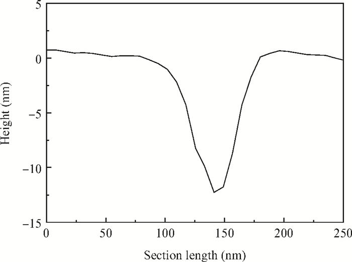
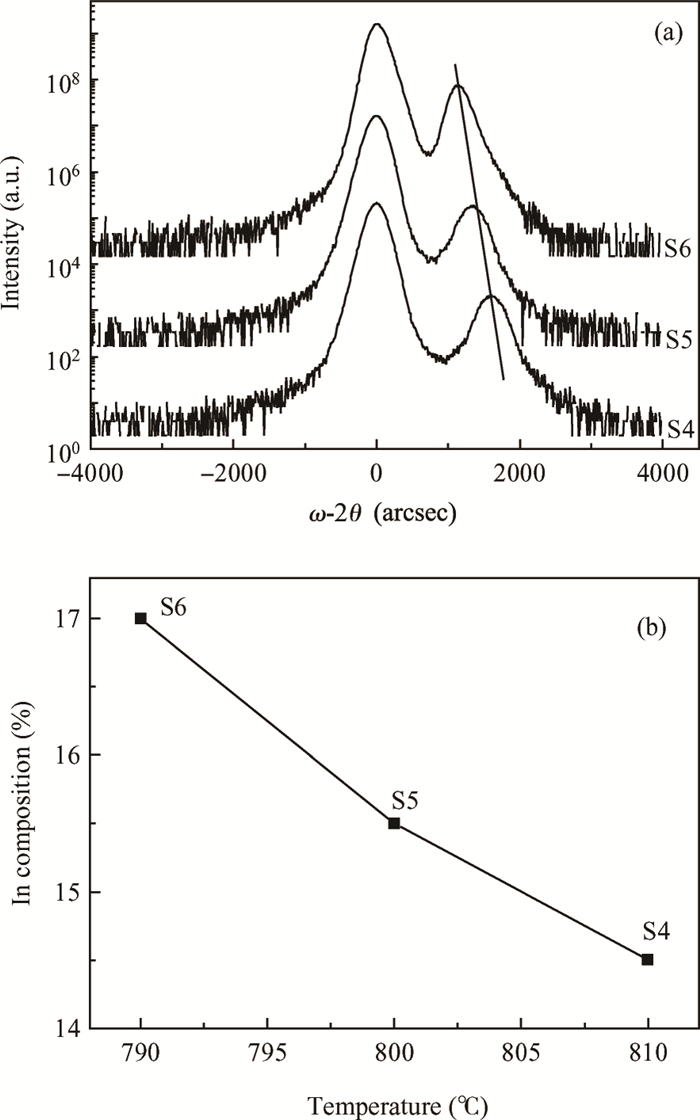
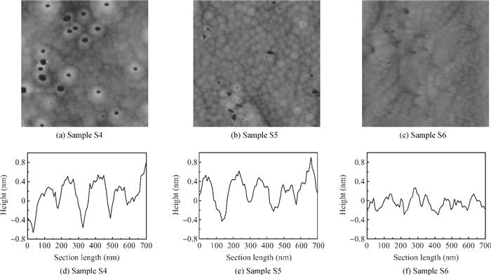
Abstract: InAlN/GaN heterostructures were grown on sapphire substrates by low-pressure metal organic chemical vapor deposition. The influences of NH3 flux and growth temperature on the In composition and morphologies of the InAlN were investigated by X-ray diffraction and atomic force microscopy. It's found that the In composition increases quickly with NH3 flux decrease. But it's not sensitive to NH3 flux under higher flux. This suggests that lower NH3 flux induces a higher growth rate and an enhanced In incorporation. The In composition also increases with the growth temperatures decreasing, and the defects of the InAlN have close relation with In composition. Unstrained InAlN with In composition of 17% is obtained at NH3 flux of 500 sccm and growth temperature of 790℃. The InAlN/GaN heterostructure high electron mobility transistor sample showed a high two-dimensional electron gas (2DEG) mobility of 1210 cm2/(V·s) with the sheet density of 2.3×1013 cm-2 at room temperature.
Keywords: InAlN, MOCVD, unstrained, mobility
| [1] |
Ciccognani W, Dominicis M D, Ferrari M, et al. High-power monolithic AlGaN/GaN HEMT switch for X-band applications. IEEE Electron Lett, 2008, 44:55 doi: 10.1049/el:20082131
|
| [2] |
Chung J W, Zhao X, Wu Y R, et al. Effect of image charges in the drain delay of AlGaN/GaN high electron mobility transistors. Appl Phys Lett, 2008, 92:093502 doi: 10.1063/1.2889498
|
| [3] |
Gonschorek M, Carlin J F, Feltin E, et al. High electron mobility lattice-matched AlInN/GaN field-effect transistor heterostructures. Appl Phys Lett, 2006, 89:062106. doi: 10.1063/1.2335390
|
| [4] |
Kuzmik J. Power electronics on InAlN/(In)GaN:prospect for a record performance. IEEE Device Lett, 2001, 22:510 doi: 10.1109/55.962646
|
| [5] |
Gonschorek M, Carlin J F, Feltin E, et al. Two-dimensional electron gas density in Al1-xInxN/AlN/GaN heterostructures (0.03≤ x ≤ 0.23). J Appl Phys, 2008, 103:093714 doi: 10.1063/1.2917290
|
| [6] |
Liu Bo, Feng Zhihong, Dun Shaobo, et al. An extrinsic fmax > 100 GHz InAlN/GaN HEMT with AlGaN back barrier. Journal of Semiconductors, 2013, 34:044006 doi: 10.1088/1674-4926/34/4/044006
|
| [7] |
Song Xubo, Gu Guodong, Dun Shaobo, et al. DC and RF characteristics of enhancement-mode InAlN/GaN HEMT with fluorine treatment. Journal of Semiconductors, 2014, 35:044002 doi: 10.1088/1674-4926/35/4/044002
|
| [8] |
Higashiwaki M, Matsui T. InAlN/GaN heterostructure field-effect transistors grown by plasma-assisted molecular-beam epitaxy. Jpn J Appl Phy., 2004, 43:L768 doi: 10.1143/JJAP.43.L768
|
| [9] |
Dadgar A, Schulze F, Blasing J, et al. High-sheet-charge-carrier-density AlInN/GaN field-effect transistors on Si (111). Appl Phys Lett, 2004, 85:5400 doi: 10.1063/1.1828580
|
| [10] |
Katz O, Mistele D, Meyler B, et al. InAlN/GaN heterostructure field-effect transistor DC and small signal characteristics. Electron Lett, 2004, 40:1304 doi: 10.1049/el:20045980
|
| [11] |
Liu Bo, Feng Zhihong, Zhang Sen, et al. A 4.69-W/mm output power density InAlN/GaN HEMT grown on sapphire substrate. Journal of Semiconductors, 2011, 32:124003 doi: 10.1088/1674-4926/32/12/124003
|
| [12] |
Lobanova A V, Mazaev K M, Talalaev R A, et al. Effect of Ⅴ/Ⅲ ratio in AlN and AlGaN MOVPE. J Cryst Growth, 2006, 287:601 doi: 10.1016/j.jcrysgro.2005.10.083
|
| [13] |
Schenk H P D, Nemoz M, Korytov M, et al. Indium incorporation dynamics into AⅡnN ternary alloys for laser structures lattice matched to GaN. Appl Phys Lett, 2008, 93:081116 doi: 10.1063/1.2971027
|
| [14] |
Choi S, Kim T H, Wolter S, et al. Indium adlayer kinetics on the gallium nitride (0001) surface:Monitoring indium segregation and precursor-mediated adsorption. Phys Rev B, 2008, 77:115435 doi: 10.1103/PhysRevB.77.115435
|
| [15] |
Kehagias T, Dimitrakopulos G P, Kioseoglou J, et al. Indium migration paths in V-defects of InAlN grown by metal-organic vapor phase epitaxy. Appl Phys Lett, 2009, 95:071905 doi: 10.1063/1.3204454
|


Article views: 3970 Times PDF downloads: 16 Times Cited by: 0 Times
Received: 31 March 2014 Revised: 21 May 2014 Online: Published: 01 November 2014
| Citation: |
Bo Liu, Jiayun Yin, Yuanjie Lü, Shaobo Dun, Xiongwen Zhang, Zhihong Feng, Shujun Cai. Unstrained InAlN/GaN heterostructures grown on sapphire substrates by MOCVD[J]. Journal of Semiconductors, 2014, 35(11): 113005. doi: 10.1088/1674-4926/35/11/113005
****
B Liu, J Y Yin, Y J Lü, S B Dun, X W Zhang, Z H Feng, S J Cai. Unstrained InAlN/GaN heterostructures grown on sapphire substrates by MOCVD[J]. J. Semicond., 2014, 35(11): 113005. doi: 10.1088/1674-4926/35/11/113005.

|
| [1] |
Ciccognani W, Dominicis M D, Ferrari M, et al. High-power monolithic AlGaN/GaN HEMT switch for X-band applications. IEEE Electron Lett, 2008, 44:55 doi: 10.1049/el:20082131
|
| [2] |
Chung J W, Zhao X, Wu Y R, et al. Effect of image charges in the drain delay of AlGaN/GaN high electron mobility transistors. Appl Phys Lett, 2008, 92:093502 doi: 10.1063/1.2889498
|
| [3] |
Gonschorek M, Carlin J F, Feltin E, et al. High electron mobility lattice-matched AlInN/GaN field-effect transistor heterostructures. Appl Phys Lett, 2006, 89:062106. doi: 10.1063/1.2335390
|
| [4] |
Kuzmik J. Power electronics on InAlN/(In)GaN:prospect for a record performance. IEEE Device Lett, 2001, 22:510 doi: 10.1109/55.962646
|
| [5] |
Gonschorek M, Carlin J F, Feltin E, et al. Two-dimensional electron gas density in Al1-xInxN/AlN/GaN heterostructures (0.03≤ x ≤ 0.23). J Appl Phys, 2008, 103:093714 doi: 10.1063/1.2917290
|
| [6] |
Liu Bo, Feng Zhihong, Dun Shaobo, et al. An extrinsic fmax > 100 GHz InAlN/GaN HEMT with AlGaN back barrier. Journal of Semiconductors, 2013, 34:044006 doi: 10.1088/1674-4926/34/4/044006
|
| [7] |
Song Xubo, Gu Guodong, Dun Shaobo, et al. DC and RF characteristics of enhancement-mode InAlN/GaN HEMT with fluorine treatment. Journal of Semiconductors, 2014, 35:044002 doi: 10.1088/1674-4926/35/4/044002
|
| [8] |
Higashiwaki M, Matsui T. InAlN/GaN heterostructure field-effect transistors grown by plasma-assisted molecular-beam epitaxy. Jpn J Appl Phy., 2004, 43:L768 doi: 10.1143/JJAP.43.L768
|
| [9] |
Dadgar A, Schulze F, Blasing J, et al. High-sheet-charge-carrier-density AlInN/GaN field-effect transistors on Si (111). Appl Phys Lett, 2004, 85:5400 doi: 10.1063/1.1828580
|
| [10] |
Katz O, Mistele D, Meyler B, et al. InAlN/GaN heterostructure field-effect transistor DC and small signal characteristics. Electron Lett, 2004, 40:1304 doi: 10.1049/el:20045980
|
| [11] |
Liu Bo, Feng Zhihong, Zhang Sen, et al. A 4.69-W/mm output power density InAlN/GaN HEMT grown on sapphire substrate. Journal of Semiconductors, 2011, 32:124003 doi: 10.1088/1674-4926/32/12/124003
|
| [12] |
Lobanova A V, Mazaev K M, Talalaev R A, et al. Effect of Ⅴ/Ⅲ ratio in AlN and AlGaN MOVPE. J Cryst Growth, 2006, 287:601 doi: 10.1016/j.jcrysgro.2005.10.083
|
| [13] |
Schenk H P D, Nemoz M, Korytov M, et al. Indium incorporation dynamics into AⅡnN ternary alloys for laser structures lattice matched to GaN. Appl Phys Lett, 2008, 93:081116 doi: 10.1063/1.2971027
|
| [14] |
Choi S, Kim T H, Wolter S, et al. Indium adlayer kinetics on the gallium nitride (0001) surface:Monitoring indium segregation and precursor-mediated adsorption. Phys Rev B, 2008, 77:115435 doi: 10.1103/PhysRevB.77.115435
|
| [15] |
Kehagias T, Dimitrakopulos G P, Kioseoglou J, et al. Indium migration paths in V-defects of InAlN grown by metal-organic vapor phase epitaxy. Appl Phys Lett, 2009, 95:071905 doi: 10.1063/1.3204454
|

 WeChat ID
Journal of Semiconductors © 2017 All Rights Reserved 京ICP备05085259号-2

 DownLoad: