


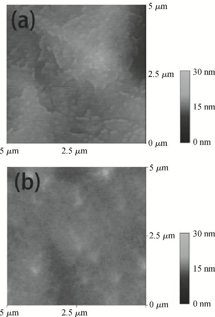
Fig. 1.
AFM images with 5 $\times $ 5 $\mu $ m$^{2}$ scans of LED samples with p-GaN grown at (a) 130 Torr and (b) 400 Torr.
SEMICONDUCTOR DEVICES
Binglei Fu, Naixin Liu, Zhe Liu, Jinmin Li and Junxi Wang
Corresponding author: Fu Binglei, Email:fubinglei@semi.ac.cn
Abstract: The advantages of InGaN/GaN light emitting diodes (LEDs) with p-GaN grown under high pressures are studied. It is shown that the high growth pressure could lead to better electronic properties of p-GaN layers due to the eliminated compensation effect. The contact resistivity of p-GaN layers are decreased due to the reduced donor-like defects on the p-GaN surface. The leakage current is also reduced, which may be induced by the better filling of V-defects with p-GaN layers grown under high pressures. The LED efficiency thus could be enhanced with high pressure grown p-GaN layers.
Keywords: light emitting diodes, V-defects, growth pressure, p-GaN
| [1] |
Meyaard D S, Lin G B, Shan Q, et al. Asymmetry of carrier transport leading to efficiency droop in GaInN based light-emitting diodes. Appl Phys Lett, 2011, 99(25):251115 doi: 10.1063/1.3671395
|
| [2] |
Le L C, Zhao D G, Jiang D S, et al. Carriers capturing of V-defect and its effect on leakage current and electroluminescence in InGaN-based light-emitting diodes. Appl Phys Lett, 2012, 101(25):252110 doi: 10.1063/1.4772548
|
| [3] |
Lee W, Limb J, Ryou J H, et al. Influence of growth temperature and growth rate of p-GaN layers on the characteristics of green light emitting diodes. J Electron Mater, 2006, 35(4):587 doi: 10.1007/s11664-006-0104-2
|
| [4] |
Fu B, Liu N, Zhang N, et al. The effect of growth pressure and growth rate on the properties of Mg-doped GaN. J Electron Mater, 2014, DOI: 10.1007/s11664-014-3005-9
|
| [5] |
Ratsch C, Garcia J, Caflisch R E. Influence of edge diffusion on the growth mode on vicinal surfaces. Appl Phys Lett, 2005, 87(14):141901 doi: 10.1063/1.2077851
|
| [6] |
Wang L C, Guo E Q, Liu Z Q, et al. Electrical characteristics of a vertical light emitting diode with n-type contacts on a selectively wet-etching roughened surface. Journal of Semiconductors, 2011, 32(2):024009 doi: 10.1088/1674-4926/32/2/024009
|
| [7] |
Liu L, Ling M, Yang J, et al. Efficiency degradation behaviors of current/thermal co-stressed GaN-based blue light emitting diodes with vertical-structure. J Appl Phys, 2012, 111(9):093110 doi: 10.1063/1.4712030
|
| [8] |
Oh M S, Kwon M K, Park I K, et al. Improvement of green LED by growing p-GaN on In0.25GaN/GaN MQWs at low temperature. J Cryst Growth, 2006, 289(1):107 doi: 10.1016/j.jcrysgro.2005.10.129
|
| [9] |
Ji Y, Zhang Z H, Kyaw Z, et al. Influence of n-type versus p-type AlGaN electron-blocking layer on InGaN/GaN multiple quantum wells light-emitting diodes. Appl Phys Lett, 2013, 103(5):053512 doi: 10.1063/1.4817381
|
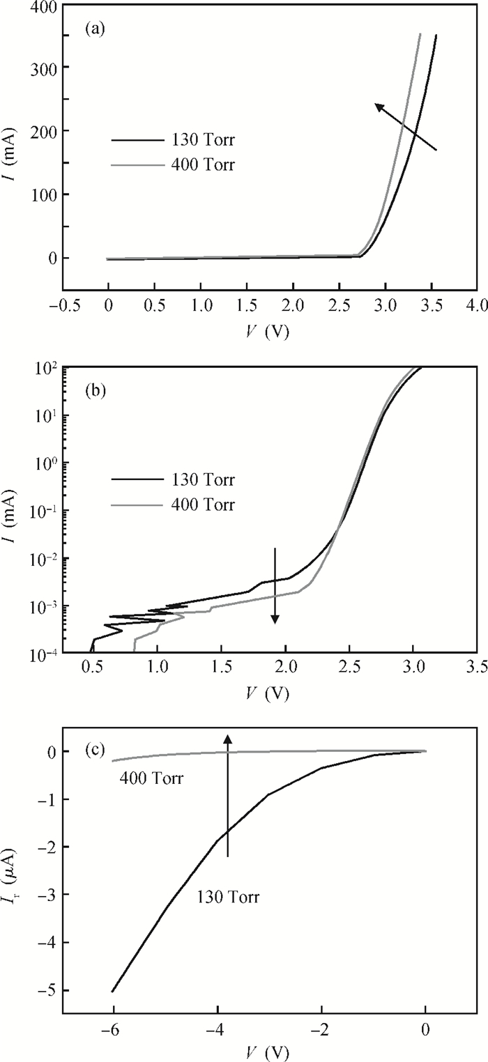
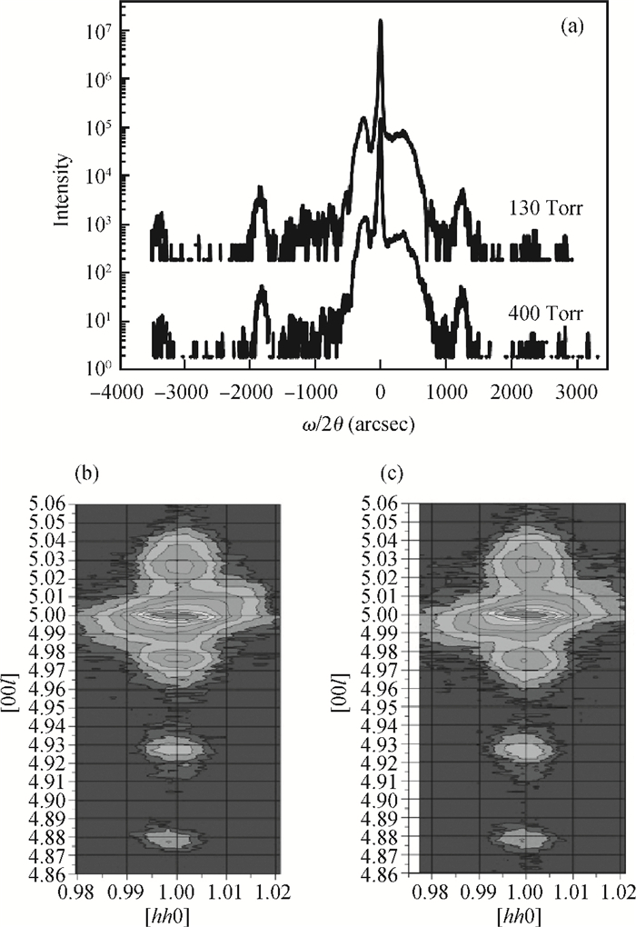

Table 1. Results of RT-Hall measurement.

|
Table 2. RSM roughness of LED surface and specific contact resistivity of ohmic contact on p-GaN.

|
| [1] |
Meyaard D S, Lin G B, Shan Q, et al. Asymmetry of carrier transport leading to efficiency droop in GaInN based light-emitting diodes. Appl Phys Lett, 2011, 99(25):251115 doi: 10.1063/1.3671395
|
| [2] |
Le L C, Zhao D G, Jiang D S, et al. Carriers capturing of V-defect and its effect on leakage current and electroluminescence in InGaN-based light-emitting diodes. Appl Phys Lett, 2012, 101(25):252110 doi: 10.1063/1.4772548
|
| [3] |
Lee W, Limb J, Ryou J H, et al. Influence of growth temperature and growth rate of p-GaN layers on the characteristics of green light emitting diodes. J Electron Mater, 2006, 35(4):587 doi: 10.1007/s11664-006-0104-2
|
| [4] |
Fu B, Liu N, Zhang N, et al. The effect of growth pressure and growth rate on the properties of Mg-doped GaN. J Electron Mater, 2014, DOI: 10.1007/s11664-014-3005-9
|
| [5] |
Ratsch C, Garcia J, Caflisch R E. Influence of edge diffusion on the growth mode on vicinal surfaces. Appl Phys Lett, 2005, 87(14):141901 doi: 10.1063/1.2077851
|
| [6] |
Wang L C, Guo E Q, Liu Z Q, et al. Electrical characteristics of a vertical light emitting diode with n-type contacts on a selectively wet-etching roughened surface. Journal of Semiconductors, 2011, 32(2):024009 doi: 10.1088/1674-4926/32/2/024009
|
| [7] |
Liu L, Ling M, Yang J, et al. Efficiency degradation behaviors of current/thermal co-stressed GaN-based blue light emitting diodes with vertical-structure. J Appl Phys, 2012, 111(9):093110 doi: 10.1063/1.4712030
|
| [8] |
Oh M S, Kwon M K, Park I K, et al. Improvement of green LED by growing p-GaN on In0.25GaN/GaN MQWs at low temperature. J Cryst Growth, 2006, 289(1):107 doi: 10.1016/j.jcrysgro.2005.10.129
|
| [9] |
Ji Y, Zhang Z H, Kyaw Z, et al. Influence of n-type versus p-type AlGaN electron-blocking layer on InGaN/GaN multiple quantum wells light-emitting diodes. Appl Phys Lett, 2013, 103(5):053512 doi: 10.1063/1.4817381
|


Article views: 3546 Times PDF downloads: 34 Times Cited by: 0 Times
Received: 21 March 2014 Revised: 06 May 2014 Online: Published: 01 November 2014
| Citation: |
Binglei Fu, Naixin Liu, Zhe Liu, Jinmin Li, Junxi Wang. Advantages of InGaN/GaN light emitting diodes with p-GaN grown under high pressure[J]. Journal of Semiconductors, 2014, 35(11): 114007. doi: 10.1088/1674-4926/35/11/114007
****
B L Fu, N X Liu, Z Liu, J M Li, J X Wang. Advantages of InGaN/GaN light emitting diodes with p-GaN grown under high pressure[J]. J. Semicond., 2014, 35(11): 114007. doi: 10.1088/1674-4926/35/11/114007.

|
| [1] |
Meyaard D S, Lin G B, Shan Q, et al. Asymmetry of carrier transport leading to efficiency droop in GaInN based light-emitting diodes. Appl Phys Lett, 2011, 99(25):251115 doi: 10.1063/1.3671395
|
| [2] |
Le L C, Zhao D G, Jiang D S, et al. Carriers capturing of V-defect and its effect on leakage current and electroluminescence in InGaN-based light-emitting diodes. Appl Phys Lett, 2012, 101(25):252110 doi: 10.1063/1.4772548
|
| [3] |
Lee W, Limb J, Ryou J H, et al. Influence of growth temperature and growth rate of p-GaN layers on the characteristics of green light emitting diodes. J Electron Mater, 2006, 35(4):587 doi: 10.1007/s11664-006-0104-2
|
| [4] |
Fu B, Liu N, Zhang N, et al. The effect of growth pressure and growth rate on the properties of Mg-doped GaN. J Electron Mater, 2014, DOI: 10.1007/s11664-014-3005-9
|
| [5] |
Ratsch C, Garcia J, Caflisch R E. Influence of edge diffusion on the growth mode on vicinal surfaces. Appl Phys Lett, 2005, 87(14):141901 doi: 10.1063/1.2077851
|
| [6] |
Wang L C, Guo E Q, Liu Z Q, et al. Electrical characteristics of a vertical light emitting diode with n-type contacts on a selectively wet-etching roughened surface. Journal of Semiconductors, 2011, 32(2):024009 doi: 10.1088/1674-4926/32/2/024009
|
| [7] |
Liu L, Ling M, Yang J, et al. Efficiency degradation behaviors of current/thermal co-stressed GaN-based blue light emitting diodes with vertical-structure. J Appl Phys, 2012, 111(9):093110 doi: 10.1063/1.4712030
|
| [8] |
Oh M S, Kwon M K, Park I K, et al. Improvement of green LED by growing p-GaN on In0.25GaN/GaN MQWs at low temperature. J Cryst Growth, 2006, 289(1):107 doi: 10.1016/j.jcrysgro.2005.10.129
|
| [9] |
Ji Y, Zhang Z H, Kyaw Z, et al. Influence of n-type versus p-type AlGaN electron-blocking layer on InGaN/GaN multiple quantum wells light-emitting diodes. Appl Phys Lett, 2013, 103(5):053512 doi: 10.1063/1.4817381
|

 WeChat ID
Journal of Semiconductors © 2017 All Rights Reserved 京ICP备05085259号-2

 DownLoad:

