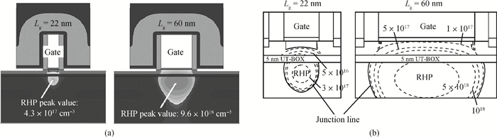
Fig. 1.
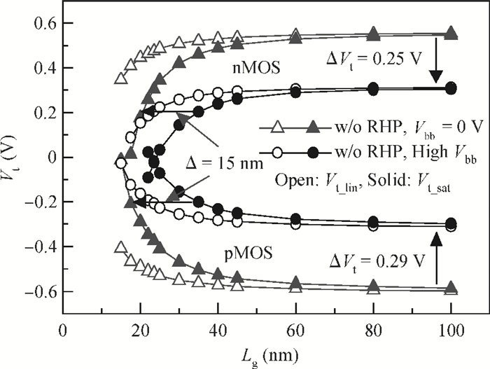
The challenges for gate length scaling with reducing $V_{\rm t}$ by adjusting back bias. $V_{\rm t-lin}$ and $V_{\rm t-sat}$ here is the threshold voltage when $V_{\rm d}$ = 0.05 V and 1 V respectively.
SEMICONDUCTOR DEVICES
Hao Wu, Miao Xu, Guangxing Wan, Huilong Zhu, Lichuan Zhao, Xiaodong Tong, Chao Zhao, Dapeng Chen and Tianchun Ye
Corresponding author: Wu Hao, Email:wuhao@ime.ac.cn; Zhu Huilong, Email:zhuhuilong@ime.ac.cn
Abstract: The importance of substrate doping engineering for extremely thin SOI MOSFETs with ultra-thin buried oxide (ES-UB-MOSFETs) is demonstrated by simulation. A new substrate/backgate doping engineering, lateral non-uniform dopant distributions (LNDD) is investigated in ES-UB-MOSFETs. The effects of LNDD on device performance, Vt-roll-off, channel mobility and random dopant fluctuation (RDF) are studied and optimized. Fixing the long channel threshold voltage (Vt) at 0.3 V, ES-UB-MOSFETs with lateral uniform doping in the substrate and forward back bias can scale only to 35 nm, meanwhile LNDD enables ES-UB-MOSFETs to scale to a 20 nm gate length, which is 43% smaller. The LNDD degradation is 10% of the carrier mobility both for nMOS and pMOS, but it is canceled out by a good short channel effect controlled by the LNDD. Fixing Vt at 0.3 V, in long channel devices, due to more channel doping concentration for the LNDD technique, the RDF in LNDD controlled ES-UB-MOSFETs is worse than in back-bias controlled ES-UB-MOSFETs, but in the short channel, the RDF for LNDD controlled ES-UB-MOSFET is better due to its self-adaption of substrate doping engineering by using a fixed thickness inner-spacer. A novel process flow to form LNDD is proposed and simulated.
Keywords: extremely thin SOI (ETSOI), fully depleted SOI (FDSOI), short channel effect ultra thin BOX (UTBOX)
| [1] |
Cheng K, Khakifirooz A, Kulkarni P, et al. Fully depleted extremely thin SOI technology fabricated by a novel integration scheme featuring implant-free, zero-silicon-loss, and faceted raised source/drain. Symp VLSI Tech, 2009:212 http://ieeexplore.ieee.org/xpls/abs_all.jsp?arnumber=5200603
|
| [2] |
Cheng K, Khakifirooz A, Kulkarni P, et al. Extremely thin SOI (ETSOI) CMOS with record low variability for low power system-on-chip applications. IEDM Tech Dig, 2009:49 http://ieeexplore.ieee.org/xpls/icp.jsp?arnumber=5424422
|
| [3] |
Fenouillet-Beranger C, Perreau P, Denorme S, et al. Impact of a 10 nm ultra-thin BOX (UTBOX) and ground plane on FDSOI devices for 32 nm node and below. ESSDERC, 2009:89 http://ieeexplore.ieee.org/xpls/icp.jsp?arnumber=5325994
|
| [4] |
TCAD Sentaurus User Manual, D-2010. 12. , Synopsys
|
| [5] |
Barral V, Poiroux T, Andrieu F, et al. Strained FDSOI CMOS technology scalability down to 2.5 nm film thickness and 18 nm gate length with a TiN/HfO2 gate stack. IEDM Tech Dig, 2007:61 http://ieeexplore.ieee.org/xpls/abs_all.jsp?arnumber=4418863
|
| [6] |
Packan P, Akbar S, Armstrong M, et al. High performance 32 nm logic technology featuring 2nd generation high-k + metal gate transistors. IEDM Tech Dig, 2009:41 http://ieeexplore.ieee.org/xpls/icp.jsp?arnumber=5424253
|
| [7] |
Andrieu F, Faynot O, Garros X, et al. Comparative scalability of PVD and CVD TiN on HfO2 as a metal gate stack for FDSOI CMOSFETs down to 25 nm gate length and width. IEDM Tech Dig, 2006:23.7 http://ieeexplore.ieee.org/xpls/icp.jsp?arnumber=4154284
|
| [8] |
Wettstein A, Penzin O, Lyumkis E, et al. Random dopant fluctuation modelling with the impedance field method. SISPAD, Boston, MA, USA, 2003:91 http://ieeexplore.ieee.org/xpls/icp.jsp?arnumber=1233645
|
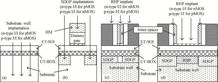
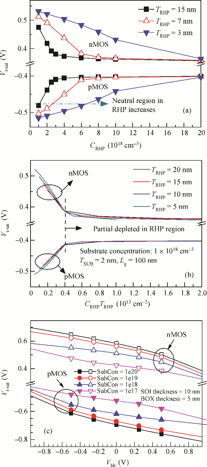
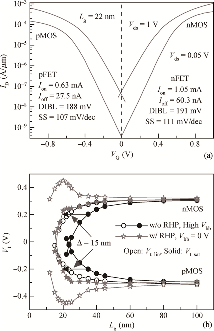
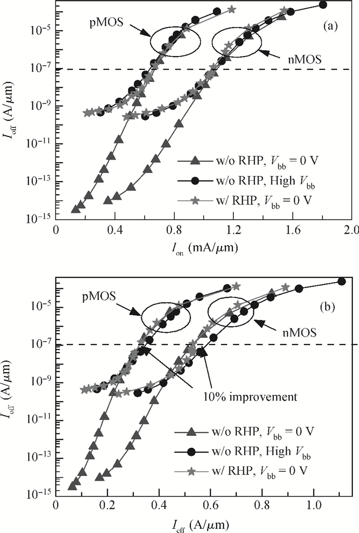
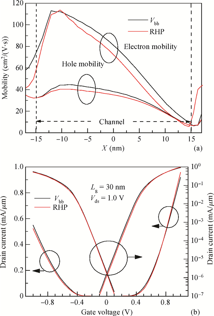
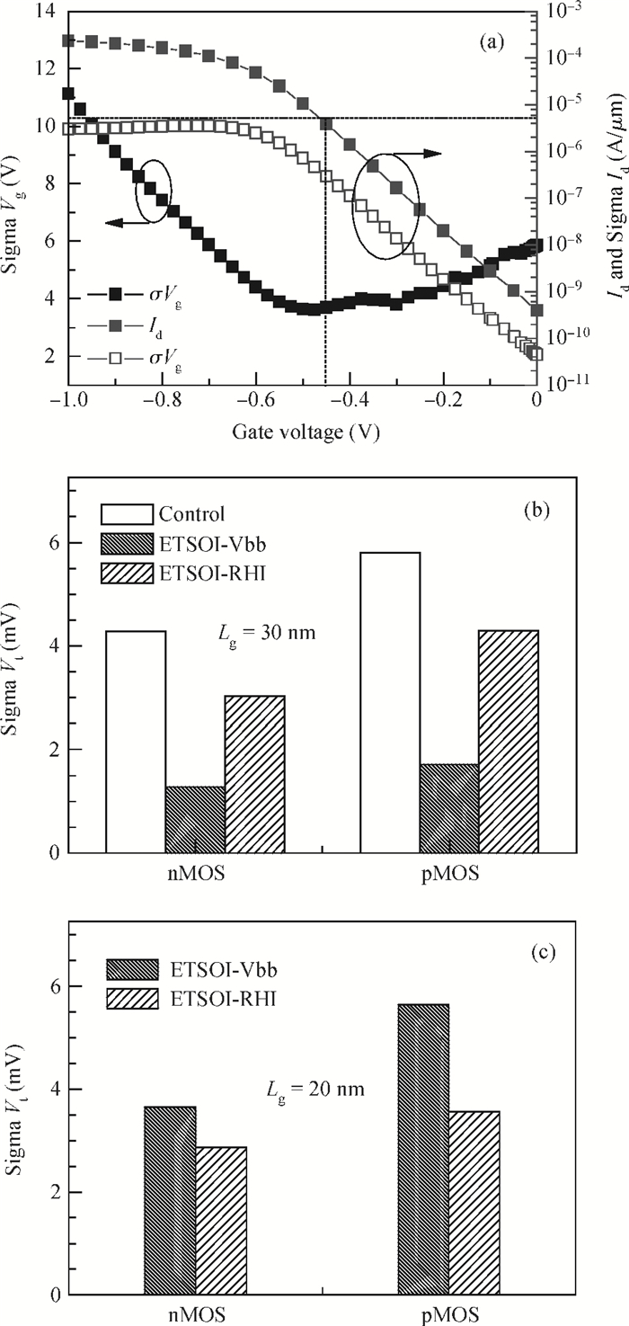
Table 1. Device parameters used in simulation.

|
| [1] |
Cheng K, Khakifirooz A, Kulkarni P, et al. Fully depleted extremely thin SOI technology fabricated by a novel integration scheme featuring implant-free, zero-silicon-loss, and faceted raised source/drain. Symp VLSI Tech, 2009:212 http://ieeexplore.ieee.org/xpls/abs_all.jsp?arnumber=5200603
|
| [2] |
Cheng K, Khakifirooz A, Kulkarni P, et al. Extremely thin SOI (ETSOI) CMOS with record low variability for low power system-on-chip applications. IEDM Tech Dig, 2009:49 http://ieeexplore.ieee.org/xpls/icp.jsp?arnumber=5424422
|
| [3] |
Fenouillet-Beranger C, Perreau P, Denorme S, et al. Impact of a 10 nm ultra-thin BOX (UTBOX) and ground plane on FDSOI devices for 32 nm node and below. ESSDERC, 2009:89 http://ieeexplore.ieee.org/xpls/icp.jsp?arnumber=5325994
|
| [4] |
TCAD Sentaurus User Manual, D-2010. 12. , Synopsys
|
| [5] |
Barral V, Poiroux T, Andrieu F, et al. Strained FDSOI CMOS technology scalability down to 2.5 nm film thickness and 18 nm gate length with a TiN/HfO2 gate stack. IEDM Tech Dig, 2007:61 http://ieeexplore.ieee.org/xpls/abs_all.jsp?arnumber=4418863
|
| [6] |
Packan P, Akbar S, Armstrong M, et al. High performance 32 nm logic technology featuring 2nd generation high-k + metal gate transistors. IEDM Tech Dig, 2009:41 http://ieeexplore.ieee.org/xpls/icp.jsp?arnumber=5424253
|
| [7] |
Andrieu F, Faynot O, Garros X, et al. Comparative scalability of PVD and CVD TiN on HfO2 as a metal gate stack for FDSOI CMOSFETs down to 25 nm gate length and width. IEDM Tech Dig, 2006:23.7 http://ieeexplore.ieee.org/xpls/icp.jsp?arnumber=4154284
|
| [8] |
Wettstein A, Penzin O, Lyumkis E, et al. Random dopant fluctuation modelling with the impedance field method. SISPAD, Boston, MA, USA, 2003:91 http://ieeexplore.ieee.org/xpls/icp.jsp?arnumber=1233645
|


Article views: 3194 Times PDF downloads: 20 Times Cited by: 0 Times
Received: 21 April 2014 Revised: 06 May 2014 Online: Published: 01 November 2014
| Citation: |
Hao Wu, Miao Xu, Guangxing Wan, Huilong Zhu, Lichuan Zhao, Xiaodong Tong, Chao Zhao, Dapeng Chen, Tianchun Ye. On substrate dopant engineering for ET-SOI MOSFETs with UT-BOX[J]. Journal of Semiconductors, 2014, 35(11): 114006. doi: 10.1088/1674-4926/35/11/114006
****
H Wu, M Xu, G X Wan, H L Zhu, L C Zhao, X D Tong, C Zhao, D P Chen, T C Ye. On substrate dopant engineering for ET-SOI MOSFETs with UT-BOX[J]. J. Semicond., 2014, 35(11): 114006. doi: 10.1088/1674-4926/35/11/114006.

|
| [1] |
Cheng K, Khakifirooz A, Kulkarni P, et al. Fully depleted extremely thin SOI technology fabricated by a novel integration scheme featuring implant-free, zero-silicon-loss, and faceted raised source/drain. Symp VLSI Tech, 2009:212 http://ieeexplore.ieee.org/xpls/abs_all.jsp?arnumber=5200603
|
| [2] |
Cheng K, Khakifirooz A, Kulkarni P, et al. Extremely thin SOI (ETSOI) CMOS with record low variability for low power system-on-chip applications. IEDM Tech Dig, 2009:49 http://ieeexplore.ieee.org/xpls/icp.jsp?arnumber=5424422
|
| [3] |
Fenouillet-Beranger C, Perreau P, Denorme S, et al. Impact of a 10 nm ultra-thin BOX (UTBOX) and ground plane on FDSOI devices for 32 nm node and below. ESSDERC, 2009:89 http://ieeexplore.ieee.org/xpls/icp.jsp?arnumber=5325994
|
| [4] |
TCAD Sentaurus User Manual, D-2010. 12. , Synopsys
|
| [5] |
Barral V, Poiroux T, Andrieu F, et al. Strained FDSOI CMOS technology scalability down to 2.5 nm film thickness and 18 nm gate length with a TiN/HfO2 gate stack. IEDM Tech Dig, 2007:61 http://ieeexplore.ieee.org/xpls/abs_all.jsp?arnumber=4418863
|
| [6] |
Packan P, Akbar S, Armstrong M, et al. High performance 32 nm logic technology featuring 2nd generation high-k + metal gate transistors. IEDM Tech Dig, 2009:41 http://ieeexplore.ieee.org/xpls/icp.jsp?arnumber=5424253
|
| [7] |
Andrieu F, Faynot O, Garros X, et al. Comparative scalability of PVD and CVD TiN on HfO2 as a metal gate stack for FDSOI CMOSFETs down to 25 nm gate length and width. IEDM Tech Dig, 2006:23.7 http://ieeexplore.ieee.org/xpls/icp.jsp?arnumber=4154284
|
| [8] |
Wettstein A, Penzin O, Lyumkis E, et al. Random dopant fluctuation modelling with the impedance field method. SISPAD, Boston, MA, USA, 2003:91 http://ieeexplore.ieee.org/xpls/icp.jsp?arnumber=1233645
|

 WeChat ID
Journal of Semiconductors © 2017 All Rights Reserved 京ICP备05085259号-2

 DownLoad: