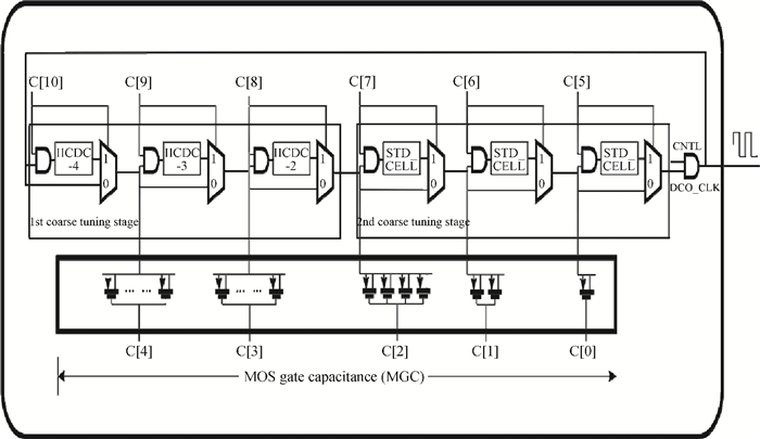
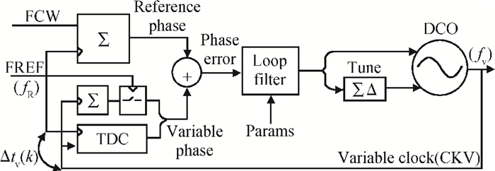
Processing math: 100%
J. Semicond. > 2014, Volume 35 > Issue 11 > 115004

SEMICONDUCTOR INTEGRATED CIRCUITS

A low-power DCO using inverter interlaced cascaded delay cell

Qiang Huang, Tao Fan, Xiangming Dai and Guoshun Yuan

+ Author Affiliations

 Corresponding author: Huang Qiang, Email:hq0817@hotmail.com

DOI: 10.1088/1674-4926/35/11/115004

PDF

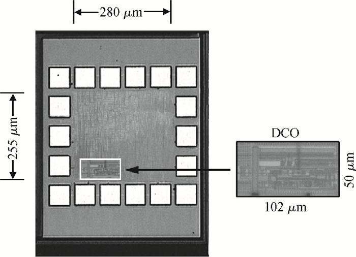
Abstract: This paper presents a low-power small-area digitally controlled oscillator (DCO) using an inverters interlaced cascaded delay cell (IICDC). It uses a coarse-fine architecture with binary-weighted delay stages for the delay range and resolution. The coarse-tuning stage of the DCO uses IICDC, which is power and area efficient with low phase noise, as compared with conventional delay cells. The ADPLL with a DCO is fabricated in the UMC 180-nm CMOS process with an active area of 0.071 mm2. The output frequency range is 140-600 MHz at the power supply of 1.8 V. The power consumption is 2.34 mW@a 200 MHz output.

Key words: all digital PLLDCOinverter interlaced cascaded delay celllow powerphase noise

All digital phase-locked loops (ADPLLs) are widely used in the on-chip clock generators. The common architecture of a DCO consists of a digitally controlled oscillator, a frequency divider, a phase frequency detector and a controller, as shown in Fig. 1[1]. The definition and operation of functional blocks have become very convenient nowadays due to digital circuit implementation. Delay, area and power consumption have kept on reducing while the process technology is scaling down. The performance of ADPLLs is improved a great deal under deep submicron technology and nanometer technology[2].

Figure  1.  Architecture diagram of ADPLL.

The DCO is the most important component of ADPLL and dominates the performance of ADPLL. The function of the DCO is to generate a clock signal whose frequency is proportional to the digital control code. A DCO is very similar to a voltage controlled oscillator except that the DCO's frequency is tuned digitally while the VCO's frequency is tuned by an analog signal[3]. As the scaling down of the process technology, a higher frequency can be generated after using fine-tuning delay cells. But in real applications, DCO delay may not meet the specified target with a large frequency range when working on the mid-low frequency or wideband frequency. An easy way to increase the coverage is by adding delay cells, but this will increase the area and leakage current significantly. Another way to achieve this, which can save the area, is dividing the high frequency signals. But the adjustable resolution is very limited with this method. So the multi-stage coarse-fine DCO architecture is commonly used to meet the frequency range and resolution requirements[4-9].

The coarse-fine DCO architecture can use large coarse delay units to increase the period range effectively. Cascaded hysteresis delay cells (CHDC)[8] are proposed for large delay generation with a relatively low power consumption and small area. Compared with traditional methods using buffers[4, 6] and logic gates[5, 7, 9], the power consumption and area are greatly reduced. However, some internal nodes in this design are weakly driven, and the process, voltage and temperature (PVT) variations of the CHDC delay cell are high. In order to guarantee a continuous period change, the fine-tuning stage should cover a wider range, so that more power and area will be consumed. Interlaced hysteresis delay cells (IHDC)[10] are proposed to get very large delays while the power is low and the area is small. The delay is generated through the signals interleaving changed between the two series of transistors. The benefit of this design is to avoid a short current and use a shared path to save leakage current. In addition to this, the internal nodes are all rail to rail so that PVT variations are reduced. However, the power consumption and phase noise of the IHDC still have the potential for optimization.

A DCO using inverters interlaced cascaded as delay cell (IICDC) is proposed in this article to get more timing delays while keeping the very low power consumption and small area. Compared with IHDC[10], our design also uses interleaving changed signals between two serials of transistors to generate the delay with the benefits of short current prevention, leakage current saving by path sharing, rail-to-rail internals nodes, and small PVT variations. The most important point is that the power consumption is greatly lowered while the phase noise is still low.

The overall architecture of the DCO is shown in Fig. 2[11]. The coarse-fine architecture is used with two stages of coarse tuning and one stage of fine tuning, which is controlled by an 11 bits period code. A binary-weighted control structure is used for both course tuning and fine tuning, which means the delay of the later stage is half of the previous stage.

Figure  2.  Architecture of the proposed DCO.

The control code of the coarse tuning stage uses a multiplexer to decide whether or not the controlled delay will be applied to the oscillation loop. The delay unit of the second coarse tuning stage is the IICDC, which will generate most of the delay. Compared with the conventional delay cell, the IICDC can provide more timing delay while consuming lower power, a smaller area and generating lower phase noise. The delay cell structure will be discussed in detail in the following section.

The fine-tuning stage is regulated by the digital controlled varactors (DCV) on the delay path. The load of varactors could be selected by the fine-tuning control code to adjust the delay of the path. The method has high resolution and good linearity. The decoder could be eliminated after using the binary-weighted code control structure.

The circuit configuration of IICDC-2 is shown in Fig. 3. The delay of the circuit is achieved by the two series of cascade pMOS and nMOS transistors (M1-M8). The nodes marked by the same characters such as A, B, C are connected together. The connections of these nodes are not drawn in order to keep the diagram clear and clean. The IICDC-2 operation timing diagram is illustrated in Fig. 4. Supposing the initial voltage at node IN is high. After IN goes to low, M1 is turned on and node A is pulled to the high voltage. M8 is turned on due to the high voltage at nodes A and B, which is discharged to low voltage. After this, M2 is turned on and node C is charged into high voltage, which will turn on M7 and force node OUT to be low. In summary, the falling edge of the signal at node IN will propagate through M1, M8, M2 and M7 to node OUT. Similarly, the rising edge at node IN will pass through M5, M3, and M6 to node OUT. From these analyses, the delay path is interlaced between these two series of cascaded transistors. The drain node of M1 is connected to the drain node of M4 through node A to avoid the weakly driven status. Similarly, M5 and M8 are connected through node B to ensure they could be charged or discharged to a stable status. So the voltage swing of all the internal nodes is rail to rail.

Figure  3.  Architecture of the proposed IICDC-2.
Figure  4.  Timing diagram of the internal nodes of IICDC-2.

As displayed in the IICDC circuit structure, pMOS and nMOS are turned on and off one after another in different paths, so no short current exists. As the delay cells are based on an inverter and the signals take a long time to propagate through, the short current is the main power consumption of this structure. In addition to this, there are only two power related paths between the power supply and the ground. The transistors on the same path have the leakage charge sharing effect to limit the leakage current. So the more transistors cascaded in the same path, the more leakage power could be saved. Due to the perfect symmetry of the interlaced structure, the design with more cascaded transistors could be easily achieved, which is shown in Figs. 5 and 6 about the design of IICDC-3 and IICDC-4.

Figure  5.  Architecture of the proposed IICDC-3.
Figure  6.  Architecture of the proposed IICDC-4.

We have made a comparison between the IHDC and our designed IICDC delay cells using 0.18 μm process technology simulation results. The delay cells are connected into ring oscillators. The number of delay cells is tuned to keep the frequency at 100 MHz. The Cadence Spectre Circuit Simulator is used for the simulation and the errpreset parameter is set to conservative.

The architecture of the IHDC delay cell[10] is shown in Fig. 7 and the measurement of the IHDC unit transient simulation results at nodes a, c, e is displayed in Fig. 8. It is notable of node d in the second stage that a path exists from the power supply to the ground, which happens at around 89 ns. Therefore, the power consumption will be increased due to the short current. To be specific, around 89 ns, node e is low and pMOS is on. Node c is high and nMOS M8 is on. At the same time, node a is high and nMOS M12 is also on. Hence the power supply is connected to the ground through M9, M8 and M12. Current will go through this path within an approximate 0.5 ns and this current does not charge or discharge any related nodes. So this portion of the power is wasted and does not contribute to the delay function of the circuit.

Figure  7.  Architecture of the IHDC-LV2.
Figure  8.  Transient simulation of the IHDC-LV2.

At the same time, from the transient simulation of the IICDC unit, which is shown in Fig. 9, there are two transistors (pMOS and nMOS) on the power supply to the ground path and these two transistors will not be on at the same time. So there is no direct path from the power supply to the ground and all the currents are used for charging and discharging the capacitor of the internal nodes. That is to say, the power efficiency is very high and the overall power consumption is very low.

Figure  9.  Transient simulation of the IICDC.

For a ring oscillator, assuming it is a liner system, the overall phase change can be calculated from the superposition principle, which is shown in Eq. (1)[12].

ϕ(t)=1qmaxti(τ)[N1n=0Γ(ω0τ+2πnN)]dτ.

(1)

In the equation, qmax is the maximum charge change of the capacitor. Γ is the impact sensitivity function (ISF). i(τ) is the total noise current injection.

Regarding Γ(ω0τ+2πnN), it could be approximated by a triangle[13], which is shown in Fig. 10. The root mean square of Γ could be calculated by the following Eq. (2).

Γ2rms=13π(1frise)3(1+A3).

(2)
Figure  10.  Derivation of the ISF approximate solution of ring oscillator.

In Eq. (2), frise and ffall are the maximum slopes of the rising edge and falling edge. A is the ratio of frise and ffall.

From the analysis above, phase change is mainly dependent on the total noise current of the node i(τ) ISF and stage number N of the ring oscillator. So the phase noise could be reduced from these three aspects.

The analysis of noise current i(τ) comes first. From the architecture of IICDC, which is illustrated in Figs. 3, 5, and 6 and the architecture of IHDC[10], the total noise current of the internal nodes is mainly from the noise of the transistors. So the noise is proportional to the number of transistors, assuming the transistors are the same size. Therefore, the noise current of IICDC-4 is approximately 57% of IHDC-LV4.

Second, in regard to ISF, which is shown in Eq. (2), the frise of the internal nodes in IICDC-4 is one time faster than IHDC-LV4 and the ffall of IICDC is also around 20% faster, which can be seen from Fig. 11. In Eq. (2), A is the ratio of frise and ffall, as frise is much smaller than ffall, so the third power of A is much smaller than 1 and can be ignored in Eq. (2). Therefore, Γ2rms is approximately proportional to (1frise)2. After an easy calculation based on the data in Fig. 11, the Γ2rms of IICDC is only 1/8 of IHDC. Hence ISF is reduced by (1n)1/2.

Figure  11.  Wave forms of ring oscillator output using (a) IHDC-LV4 and (b) IICDC-4 separately.

Third, when it comes the stage number N of the ring oscillator, since the delay of IICDC is smaller than IHDC, the number N of IICDC-4 will be almost doubled in simulation compared to IHDC-LV4.

From the discussion of these three aspects above, it can be calculated from Eq. (1) that ϕ(t) of IICDC-4 is around one fifth of IHDC-LV4.

According to the simulation results in Table 1, it confirms the conclusion of our theoretical analyses. IICDC has better performance on power consumption, although the area is increased slightly. In regard to the phase noise, there is deviation between the simulation results and theoretical analyses above due to the approximate calculation and some ignored factors. It still shows that the phase noise is greatly improved in IICDC.

Table  1.  Delay cell comparisons.
DownLoad: CSV  | Show Table

The ADPLL is implemented using the architecture in Fig. 1 and fabricated by UMC 0.18 μm RF 1P6M technology. DCO is designed with the architecture in Fig. 2. Figure 13 is the snapshot of the chip. The total area of the ADPLL chip is 0.071 mm2 and the area of the DCO is 0.0051 mm2. The core power supple voltage is 1.8 V. When the ADPLL is working at 200 MHz, the power consumption is 2.34 mW based on the current measurement and the RMS period jitter is 42 ps measured by the Agilent oscilloscope, which is shown in Fig. 12. The output frequency of the ADPLL is from 140 to 600 MHz. A comparison among several designs is shown in Table 2. The measurement results of the delay range and step resolution are listed in Table 3.

Figure  13.  Chip photomicrograph.
Figure  12.  Measured waveform and period of the ADPLL output at 200 MHz.
Table  2.  Performance comparison.
DownLoad: CSV  | Show Table
Table  3.  Measured delay range and step resolution of the tuning stages.
DownLoad: CSV  | Show Table

From the data in Table 2, our design consumes more power and area than Ref.[10] because of the process technology difference and the complex design of the control loop.

From the discussion in Section 3, IICDC consumes less power than IHDC while getting the same timing delay. In addition to this, the phase noise of IICDC is also better than IHDC. From the data in Table 2, our ADPLL design using the IICDC structure has better RMS period jitter than IHDC. However, the area and power are higher than IHDC due to the following reasons:

(1) The process technology is different. Area usage and power consumption will benefit from smaller process technology. (2) The other blocks in our ADPLL design are very complex and consume more power and area. (3) The number of IICDC units used in this design is relatively small. So the advantage of power consumption could not be shown well. (4) In spite of the impact of the layout design, parasitic effect and other non-ideal factors, the RMS period jitter of IICDC is still improved.

This paper introduces a novel design of an inverter interlaced cascaded delay cell (IICDC) with low power, low phase noise and small area. The low power and low phase noise benefits are also analyzed in detail. The ADPLL using the IICDC cells is designed and fabricated by UMC 0.18 μm process technology. The measurement results show that the full chip power consumption is 2.34 mW at 200 MHz and the RMS period jitter is 42 ps. The results illustrate that using the IICDC design as delay cells can largely improve the power consumption and phase noise under low frequency and a wide period range.


[1]
Zhuang J, Staszewski R B. A low-power all-digital PLL architecture based on phase prediction. IEEE International Conference on Electronics, Circuits and Systems, 2012:797 http://ieeexplore.ieee.org/xpls/icp.jsp?arnumber=6463539
[2]
Staszewski R B. State-of-the-art and future directions of high performance all-digital frequency synthesis in nanometer CMOS. IEEE Trans Circuits Syst Ⅰ, Reg Papers, 2011, 58(7):1497 doi: 10.1109/TCSI.2011.2150890
[3]
Tian Huanhuan, Li Zhiqiang, Chen Pufeng, et al. A low-power and low-phase-noise LC digitally controlled oscillator featuring a novel capacitor bank. Journal of Semiconductors, 2010, 31(12):125003 doi: 10.1088/1674-4926/31/12/125003
[4]
Chung C C, Lee C Y. An all-digital phase-locked loop for high speed clock generation. IEEE J Solid-State Circuits, 2003, 38(2):347 doi: 10.1109/JSSC.2002.807398
[5]
Choi K H, Shin J B, Sim J Y, et al. An interpolating digitally controlled oscillator for a wide-range all-digital PLL. IEEE Trans Circuits Syst Ⅰ, Reg Papers, 2009, 56(9):2055 doi: 10.1109/TCSI.2008.2011577
[6]
Hsu H J, Huang S Y. A low-jitter ADPLL via a suppressive digital filter and an interpolation-based locking scheme. IEEE Trans Very Large Scale Integr (VLSI) Syst, 2011, 19(1):165 doi: 10.1109/TVLSI.2009.2030410
[7]
Chung C C, Ko C Y. A fast phase tracking ADPLL for video pixel clock generation in 65 nm CMOS technology. IEEE J Solid-State Circuits, 2011, 46(10):2300 doi: 10.1109/JSSC.2011.2160789
[8]
Hsu S Y, Yu J Y, Lee C Y. A sub-10μW DCO based on HDC topologies for WBAN applications. IEEE Trans Circuits Syst Ⅱ, Exp Briefs, 2010, 57(12):951 doi: 10.1109/TCSII.2010.2087991
[9]
Sheng D, Chung C C, Lee C Y. An ultra-low-power and portable digitally controlled oscillator for SoC applications. IEEE Trans Circuits Syst Ⅱ, Exp Briefs, 2007, 54(11):954 doi: 10.1109/TCSII.2007.903782
[10]
Yu C, Chung C, Yu C, et al. A low-power DCO using interlaced hysteresis delay cells. IEEE Trans Circuits Syst Ⅱ:Express Briefs, 2012, 59(10):673 doi: 10.1109/TCSII.2012.2213357
[11]
Chenguang W. Research on key techniques of all-digital clock cells in low-power high-integration transceivers. Institute of Microelectronics of Chinese Academy of Sciences, 2013
[12]
Hajimiri A, Limotyrakis S, Lee T H. Jitter and phase noise in ring oscillators. IEEE J Solid-State Circuits, 1999, 34(6):790 doi: 10.1109/4.766813
[13]
Lee T H, Yu Z P, Zhou R D. The design of CMOS radio frequency integrated circuits. 2nd ed. Publishing House of Electronics Industry, 2006:525
[14]
Liu W, Li W, Ren P, et al. A PVT tolerant 10 to 500 MHz all-digital phase-locked loop with coupled TDC and DCO. IEEE J Solid-State Circuits, 2010, 45(2):314 doi: 10.1109/JSSC.2009.2038127
[15]
Wu C T, Shen W C, Wang W, et al. A two-cycle lock-in time ADPLL design based o n a frequency estimation algorithm. IEEE Trans Circuits Syst Ⅱ, Exp Briefs, 2010, 57(6):430 doi: 10.1109/TCSII.2010.2048358
Fig. 1.  Architecture diagram of ADPLL.

Fig. 2.  Architecture of the proposed DCO.

Fig. 3.  Architecture of the proposed IICDC-2.

Fig. 4.  Timing diagram of the internal nodes of IICDC-2.

Fig. 5.  Architecture of the proposed IICDC-3.

Fig. 6.  Architecture of the proposed IICDC-4.

Fig. 7.  Architecture of the IHDC-LV2.

Fig. 8.  Transient simulation of the IHDC-LV2.

Fig. 9.  Transient simulation of the IICDC.

Fig. 10.  Derivation of the ISF approximate solution of ring oscillator.

Fig. 11.  Wave forms of ring oscillator output using (a) IHDC-LV4 and (b) IICDC-4 separately.

Fig. 13.  Chip photomicrograph.

Fig. 12.  Measured waveform and period of the ADPLL output at 200 MHz.

Table 1.   Delay cell comparisons.

Table 2.   Performance comparison.

Table 3.   Measured delay range and step resolution of the tuning stages.

[1]
Zhuang J, Staszewski R B. A low-power all-digital PLL architecture based on phase prediction. IEEE International Conference on Electronics, Circuits and Systems, 2012:797 http://ieeexplore.ieee.org/xpls/icp.jsp?arnumber=6463539
[2]
Staszewski R B. State-of-the-art and future directions of high performance all-digital frequency synthesis in nanometer CMOS. IEEE Trans Circuits Syst Ⅰ, Reg Papers, 2011, 58(7):1497 doi: 10.1109/TCSI.2011.2150890
[3]
Tian Huanhuan, Li Zhiqiang, Chen Pufeng, et al. A low-power and low-phase-noise LC digitally controlled oscillator featuring a novel capacitor bank. Journal of Semiconductors, 2010, 31(12):125003 doi: 10.1088/1674-4926/31/12/125003
[4]
Chung C C, Lee C Y. An all-digital phase-locked loop for high speed clock generation. IEEE J Solid-State Circuits, 2003, 38(2):347 doi: 10.1109/JSSC.2002.807398
[5]
Choi K H, Shin J B, Sim J Y, et al. An interpolating digitally controlled oscillator for a wide-range all-digital PLL. IEEE Trans Circuits Syst Ⅰ, Reg Papers, 2009, 56(9):2055 doi: 10.1109/TCSI.2008.2011577
[6]
Hsu H J, Huang S Y. A low-jitter ADPLL via a suppressive digital filter and an interpolation-based locking scheme. IEEE Trans Very Large Scale Integr (VLSI) Syst, 2011, 19(1):165 doi: 10.1109/TVLSI.2009.2030410
[7]
Chung C C, Ko C Y. A fast phase tracking ADPLL for video pixel clock generation in 65 nm CMOS technology. IEEE J Solid-State Circuits, 2011, 46(10):2300 doi: 10.1109/JSSC.2011.2160789
[8]
Hsu S Y, Yu J Y, Lee C Y. A sub-10μW DCO based on HDC topologies for WBAN applications. IEEE Trans Circuits Syst Ⅱ, Exp Briefs, 2010, 57(12):951 doi: 10.1109/TCSII.2010.2087991
[9]
Sheng D, Chung C C, Lee C Y. An ultra-low-power and portable digitally controlled oscillator for SoC applications. IEEE Trans Circuits Syst Ⅱ, Exp Briefs, 2007, 54(11):954 doi: 10.1109/TCSII.2007.903782
[10]
Yu C, Chung C, Yu C, et al. A low-power DCO using interlaced hysteresis delay cells. IEEE Trans Circuits Syst Ⅱ:Express Briefs, 2012, 59(10):673 doi: 10.1109/TCSII.2012.2213357
[11]
Chenguang W. Research on key techniques of all-digital clock cells in low-power high-integration transceivers. Institute of Microelectronics of Chinese Academy of Sciences, 2013
[12]
Hajimiri A, Limotyrakis S, Lee T H. Jitter and phase noise in ring oscillators. IEEE J Solid-State Circuits, 1999, 34(6):790 doi: 10.1109/4.766813
[13]
Lee T H, Yu Z P, Zhou R D. The design of CMOS radio frequency integrated circuits. 2nd ed. Publishing House of Electronics Industry, 2006:525
[14]
Liu W, Li W, Ren P, et al. A PVT tolerant 10 to 500 MHz all-digital phase-locked loop with coupled TDC and DCO. IEEE J Solid-State Circuits, 2010, 45(2):314 doi: 10.1109/JSSC.2009.2038127
[15]
Wu C T, Shen W C, Wang W, et al. A two-cycle lock-in time ADPLL design based o n a frequency estimation algorithm. IEEE Trans Circuits Syst Ⅱ, Exp Briefs, 2010, 57(6):430 doi: 10.1109/TCSII.2010.2048358
1

Experimental study on phase noise of terahertz quantum cascade laser frequency comb and dual-comb sources

Lulu Zheng, Xianglong Bi, Xuhong Ma, Guibin Liu, Binbin Liu, et al.

Journal of Semiconductors, 2024, 45(12): 122401. doi: 10.1088/1674-4926/24060028

2

An 80-GHz DCO utilizing improved SC ladder and promoted DCTL-based hybrid tuning banks

Lu Tang, Yi Chen, Kui Wang

Journal of Semiconductors, 2023, 44(10): 102402. doi: 10.1088/1674-4926/44/10/102402

3

A low phase noise and low spur PLL frequency synthesizer for GNSS receivers

Sen Li, Jinguang Jiang, Xifeng Zhou, Jianghua Liu

Journal of Semiconductors, 2014, 35(1): 015004. doi: 10.1088/1674-4926/35/1/015004

4

Phase noise modeling in LC oscillators implemented in SiGe technology

M. Bouhouche, S. Latreche, C. Gontrand

Journal of Semiconductors, 2013, 34(2): 025001. doi: 10.1088/1674-4926/34/2/025001

5

A 5 Gb/s low power current-mode transmitter with pre-emphasis for serial links

Junsheng Lü, Hao Ju, Mao Ye, Feng Zhang, Jianzhong Zhao, et al.

Journal of Semiconductors, 2013, 34(7): 075002. doi: 10.1088/1674-4926/34/7/075002

6

S-band low noise amplifier using 1 μm InGaAs/InAlAs/InP pHEMT

Z. Hamaizia, N. Sengouga, M. C. E. Yagoub, M. Missous

Journal of Semiconductors, 2012, 33(2): 025001. doi: 10.1088/1674-4926/33/2/025001

7

A 2.4 GHz high-linearity low-phase-noise CMOS LC-VCO based on capacitance compensation

Li Zhenrong, Zhuang Yiqi, Li Bing, Jin Gang, Jin Zhao, et al.

Journal of Semiconductors, 2010, 31(7): 075005. doi: 10.1088/1674-4926/31/7/075005

8

A low power automatic gain control loop for a receiver

Li Guofeng, Geng Zhiqing, Wu Nanjian

Journal of Semiconductors, 2010, 31(9): 095009. doi: 10.1088/1674-4926/31/9/095009

9

A high-performance, low-power ΣΔ ADC for digital audio applications

Luo Hao, Han Yan, Ray C. C. Cheung, Han Xiaoxia, Ma Shaoyu, et al.

Journal of Semiconductors, 2010, 31(5): 055009. doi: 10.1088/1674-4926/31/5/055009

10

A 0.18 μm CMOS dual-band low power low noise amplifier for a global navigation satellite system

Li Bing, Zhuang Yiqi, Li Zhenrong, Jin Gang

Journal of Semiconductors, 2010, 31(12): 125001. doi: 10.1088/1674-4926/31/12/125001

11

A low-power and low-phase-noise LC digitally controlled oscillator featuring a novel capacitor bank

Tian Huanhuan, Li Zhiqiang, Chen Pufeng, Wu Rufei, Zhang Haiying, et al.

Journal of Semiconductors, 2010, 31(12): 125003. doi: 10.1088/1674-4926/31/12/125003

12

A low-phase-noise digitally controlled crystal oscillator for DVB TV tuners

Zhao Wei, Lu Lei, Tang Zhangwen

Journal of Semiconductors, 2010, 31(7): 075003. doi: 10.1088/1674-4926/31/7/075003

13

A 0.5–1.7 GHz low phase noise ring-oscillator-based PLL for mixed-signal SoCs

Jiao Yishu, Zhou Yumei, Jiang Jianhua, Wu Bin

Journal of Semiconductors, 2010, 31(9): 095002. doi: 10.1088/1674-4926/31/9/095002

14

A 2.4-GHz low power dual gain low noise amplifier for ZigBee

Gao Peijun, Min Hao

Journal of Semiconductors, 2009, 30(7): 075007. doi: 10.1088/1674-4926/30/7/075007

15

A Low Noise,Low Power Fully Digitally Controlled LC Oscillator for PHS Transceivers

Wang Shaohua, Yu Guangming, Liu Yongpan, Yang Huazhong

Chinese Journal of Semiconductors , 2007, 28(11): 1836-1843.

16

Design of a Monolithic CMOS LC-Voltage Controlled Oscillator with Low Phase Noise for 4GHz Frequency Synthesizers

Tang Lu, Wang Zhigong, Huang Ting, Li Zhiqun

Chinese Journal of Semiconductors , 2006, 27(3): 459-466.

17

CMOS Implementation of a Wideband Low Phase Noise PLL Frequency Synthesizer

Chen Zuotian, Wu Xuan, Tang Shoulong, Wu Jianhui

Chinese Journal of Semiconductors , 2006, 27(10): 1838-1843.

18

A Novel Method to Compensate the Sigma-Delta Shaped Noise for Wide Band Fractional-N Frequency Synthesizers

Shi Hao, Liu Junhua, Zhang Guoyan, Liao Huailin, Huang Ru, et al.

Chinese Journal of Semiconductors , 2006, 27(4): 646-652.

19

A Low Power SRAM/SOI Memory Cell Design

Yu Yang, Zhao Qian, Shao Zhibiao

Chinese Journal of Semiconductors , 2006, 27(2): 318-322.

20

Low Phase Noise Quadrature Oscillators Using New Injection Locked Technique

Chinese Journal of Semiconductors , 2005, 26(9): 1705-1710.

  • Search

    Advanced Search >>

    GET CITATION

    Qiang Huang, Tao Fan, Xiangming Dai, Guoshun Yuan. A low-power DCO using inverter interlaced cascaded delay cell[J]. Journal of Semiconductors, 2014, 35(11): 115004. doi: 10.1088/1674-4926/35/11/115004
    Q Huang, T Fan, X M Dai, G S Yuan. A low-power DCO using inverter interlaced cascaded delay cell[J]. J. Semicond., 2014, 35(11): 115004. doi: 10.1088/1674-4926/35/11/115004.
    shu

    Export: BibTex EndNote

    Article Metrics

    Article views: 2442 Times PDF downloads: 36 Times Cited by: 0 Times

    History

    Received: 25 April 2014 Revised: 11 May 2014 Online: Published: 01 November 2014

    Catalog

      Email This Article

      User name:
      Email:*请输入正确邮箱
      Code:*验证码错误
      Qiang Huang, Tao Fan, Xiangming Dai, Guoshun Yuan. A low-power DCO using inverter interlaced cascaded delay cell[J]. Journal of Semiconductors, 2014, 35(11): 115004. doi: 10.1088/1674-4926/35/11/115004 ****Q Huang, T Fan, X M Dai, G S Yuan. A low-power DCO using inverter interlaced cascaded delay cell[J]. J. Semicond., 2014, 35(11): 115004. doi: 10.1088/1674-4926/35/11/115004.
      Citation:
      Qiang Huang, Tao Fan, Xiangming Dai, Guoshun Yuan. A low-power DCO using inverter interlaced cascaded delay cell[J]. Journal of Semiconductors, 2014, 35(11): 115004. doi: 10.1088/1674-4926/35/11/115004 ****
      Q Huang, T Fan, X M Dai, G S Yuan. A low-power DCO using inverter interlaced cascaded delay cell[J]. J. Semicond., 2014, 35(11): 115004. doi: 10.1088/1674-4926/35/11/115004.

      A low-power DCO using inverter interlaced cascaded delay cell

      DOI: 10.1088/1674-4926/35/11/115004
      More Information
      • Corresponding author: Huang Qiang, Email:hq0817@hotmail.com
      • Received Date: 2014-04-25
      • Revised Date: 2014-05-11
      • Published Date: 2014-11-01

      Catalog

        /

        DownLoad:  Full-Size Img  PowerPoint
        Return
        Return