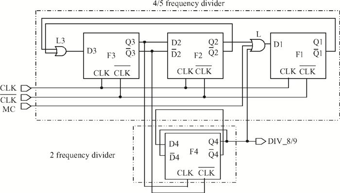
Fig. 1.
Traditional structure of 8/9 divider.
SEMICONDUCTOR INTEGRATED CIRCUITS
Zheng Sun1, Yong Xu1, , Guangyan Ma2, Hui Shi1, Fei Zhao3 and Ying Lin1
Corresponding author: Xu Yong, Email:xu_yong99@163.com
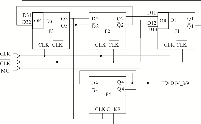
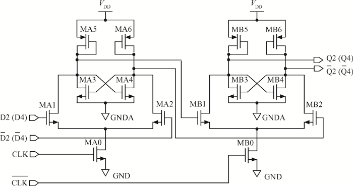
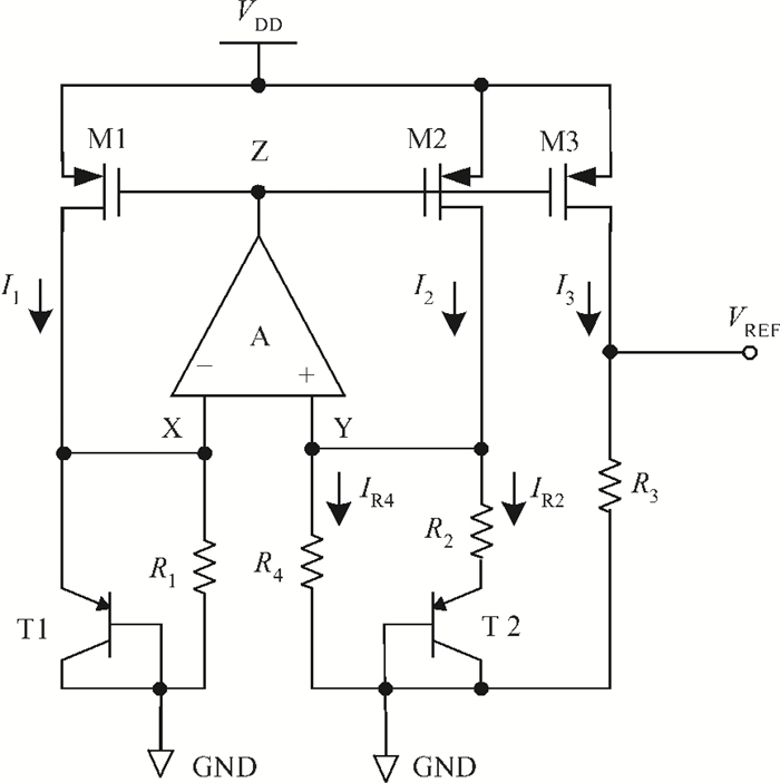
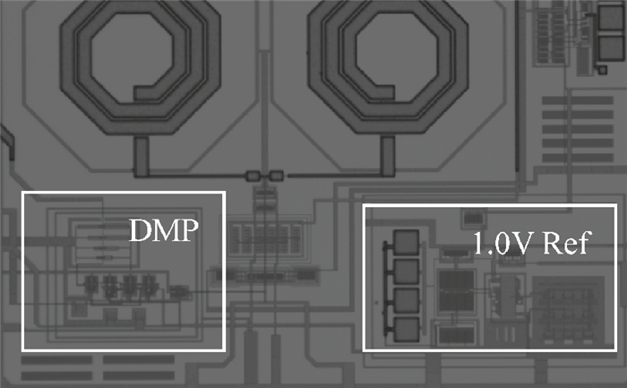
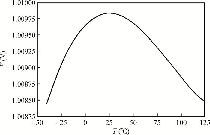
Abstract: A fully integrated 2n/2n+1 dual-modulus divider in GHz frequency range is presented. The improved structure can make all separated logic gates embed into correlative D flip-flops completely. In this way, the complex logic functions can be performed with a minimum number of devices and with maximum speed, so that lower power consumption and faster speed are obtained. In addition, the low-voltage bandgap reference needed by the frequency divider is specifically designed to provide a 1.0 V output. According to the design demand, the circuit is fabricated in 0.18 μm standard CMOS process, and the measured results show that its operating frequency range is 1.1-2.5 GHz. The dual-modulus divider dissipates 1.1 mA from a 1.8 V power supply. The temperature coefficient of the reference voltage circuit is 8.3 ppm/℃ when the temperature varies from -40 to +125℃. By comparison, the dual-modulus divide designed in this paper can possess better performance and flexibility.
Keywords: fully-integrated, dual-modulus divider, source-coupled logic (SCL), bandgap reference
| [1] |
Li Zhengrong, Zhuang Yiqi, Li Bing, et al. A 9.8-mW 1.2-GHz CMOS frequency synthesizer with a low phase-noise LC-VCO and an I/Q frequency divider. Journal of Semiconductors, 2011, 32(7):075008 doi: 10.1088/1674-4926/32/7/075008
|
| [2] |
Shu Haiyong, Li Zhiqun. A 5-GHz programmable frequency divider in 0.18-μm CMOS technology. Journal of Semiconductors, 2010, 31(5):055004 doi: 10.1088/1674-4926/31/5/055004
|
| [3] |
Guo Ting, Li Zhiqun, Li Qin, et al. A 7-27 GHz DSCL divide-by-2 frequency divider. Journal of Semiconductors, 2011, 33(10):105006 http://www.jos.ac.cn/bdtxbcn/ch/reader/view_abstract.aspx?flag=1&file_no=12030703&journal_id=bdtxbcn
|
| [4] |
Sun Yu, Mei Niansong, Lu Bo, et al. 8.64-11.62 GHz CMOS VCO and divider in a zero-IF 802.11a/b/g WLAN and Bluetooth application. Journal of Semiconductors, 2010, 31(10):105005 doi: 10.1088/1674-4926/31/10/105005
|
| [5] |
Ueno K, Hirose T, Asai T, et al. A 300 nW, 15 ppm/℃, 20 ppm/V CMOS voltage reference circuit consisting of subthreshold MOSFETs. IEEE J Solid-State Circuits, 2009, 44(7):2047 doi: 10.1109/JSSC.2009.2021922
|
| [6] |
Isikhan M, Reich T, Richter A, et al. A new low voltage bandgap reference topology. The 16th IEEE International Conference on Electronics, Circuits, and Systems, 2009:183 http://ieeexplore.ieee.org/xpls/icp.jsp?arnumber=5410966
|
| [7] |
Xing Xinpen, Li Dongmei. A near-1 V 10 ppm/℃ CMOS bandgap reference with curvature compensation. Journal of Semiconductors, 2008, 29(1):24 http://www.jos.ac.cn/bdtxbcn/ch/reader/view_abstract.aspx?flag=1&file_no=07070908&journal_id=bdtxbcn
|
| [8] |
Chao Feng, Jinhui Wang, Wei Wu, et al. CMOS 1.2 V bandgap voltage reference design. 2013 IEEE 10th International Conference on ASIC, 2013:895 http://en.cnki.com.cn/Article_en/CJFDTotal-RJZZ201405008.htm
|
| [9] |
Razavi B. Design of analog CMOS integrated circuits. Beijing:Tsinghua University Press, 2005
|
| [10] |
Li Zhiqiang, Chen Liqiang, Zhang Jian, et al. A programmable 2.4 GHz CMOS multi-modulus frequency divider. Journal of Semiconductors, 2008, 29(2):224 http://www.jos.ac.cn/bdtxbcn/ch/reader/view_abstract.aspx?flag=1&file_no=07080901&journal_id=bdtxbcn
|
| [11] |
Chen Ziyan, Chen Lei, Ma Heliang, et al. Wide band injection-locked quadrature prescaler based on ring oscillators. The 9th International Conference on Solid-State and Integrated Circuit Technology, 2008:1600 http://ieeexplore.ieee.org/document/4734866/
|
| [12] |
Guo Shita, Huang Lu, Bai Xuefei. A 4-GHz CMOS dual-modulus prescaler with enhanced input sensitivity over extended operation range. The 11th IEEE International Conference on Communication Technology, 2008:331 http://ieeexplore.ieee.org/document/4716259/
|
| [13] |
Liu Huimin, Zhang Xiaoxing, Dai Yujie, et al. Low power consumption high speed CMOS dual-modulus 15/16 prescaler for optical and wireless communications. Optoelectron Lett, 2011, 7(5):0343 http://kns.cnki.net/KCMS/detail/detail.aspx?filename=oelj201105008&dbname=CJFD&dbcode=CJFQ
|
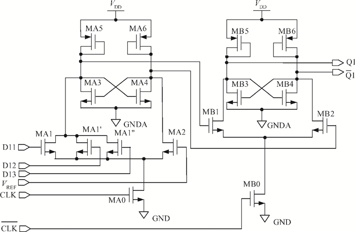

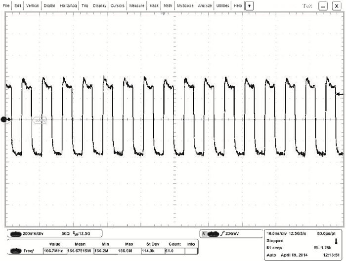
Table 1. The performance comparison with other dual-modulus dividers.

|
| [1] |
Li Zhengrong, Zhuang Yiqi, Li Bing, et al. A 9.8-mW 1.2-GHz CMOS frequency synthesizer with a low phase-noise LC-VCO and an I/Q frequency divider. Journal of Semiconductors, 2011, 32(7):075008 doi: 10.1088/1674-4926/32/7/075008
|
| [2] |
Shu Haiyong, Li Zhiqun. A 5-GHz programmable frequency divider in 0.18-μm CMOS technology. Journal of Semiconductors, 2010, 31(5):055004 doi: 10.1088/1674-4926/31/5/055004
|
| [3] |
Guo Ting, Li Zhiqun, Li Qin, et al. A 7-27 GHz DSCL divide-by-2 frequency divider. Journal of Semiconductors, 2011, 33(10):105006 http://www.jos.ac.cn/bdtxbcn/ch/reader/view_abstract.aspx?flag=1&file_no=12030703&journal_id=bdtxbcn
|
| [4] |
Sun Yu, Mei Niansong, Lu Bo, et al. 8.64-11.62 GHz CMOS VCO and divider in a zero-IF 802.11a/b/g WLAN and Bluetooth application. Journal of Semiconductors, 2010, 31(10):105005 doi: 10.1088/1674-4926/31/10/105005
|
| [5] |
Ueno K, Hirose T, Asai T, et al. A 300 nW, 15 ppm/℃, 20 ppm/V CMOS voltage reference circuit consisting of subthreshold MOSFETs. IEEE J Solid-State Circuits, 2009, 44(7):2047 doi: 10.1109/JSSC.2009.2021922
|
| [6] |
Isikhan M, Reich T, Richter A, et al. A new low voltage bandgap reference topology. The 16th IEEE International Conference on Electronics, Circuits, and Systems, 2009:183 http://ieeexplore.ieee.org/xpls/icp.jsp?arnumber=5410966
|
| [7] |
Xing Xinpen, Li Dongmei. A near-1 V 10 ppm/℃ CMOS bandgap reference with curvature compensation. Journal of Semiconductors, 2008, 29(1):24 http://www.jos.ac.cn/bdtxbcn/ch/reader/view_abstract.aspx?flag=1&file_no=07070908&journal_id=bdtxbcn
|
| [8] |
Chao Feng, Jinhui Wang, Wei Wu, et al. CMOS 1.2 V bandgap voltage reference design. 2013 IEEE 10th International Conference on ASIC, 2013:895 http://en.cnki.com.cn/Article_en/CJFDTotal-RJZZ201405008.htm
|
| [9] |
Razavi B. Design of analog CMOS integrated circuits. Beijing:Tsinghua University Press, 2005
|
| [10] |
Li Zhiqiang, Chen Liqiang, Zhang Jian, et al. A programmable 2.4 GHz CMOS multi-modulus frequency divider. Journal of Semiconductors, 2008, 29(2):224 http://www.jos.ac.cn/bdtxbcn/ch/reader/view_abstract.aspx?flag=1&file_no=07080901&journal_id=bdtxbcn
|
| [11] |
Chen Ziyan, Chen Lei, Ma Heliang, et al. Wide band injection-locked quadrature prescaler based on ring oscillators. The 9th International Conference on Solid-State and Integrated Circuit Technology, 2008:1600 http://ieeexplore.ieee.org/document/4734866/
|
| [12] |
Guo Shita, Huang Lu, Bai Xuefei. A 4-GHz CMOS dual-modulus prescaler with enhanced input sensitivity over extended operation range. The 11th IEEE International Conference on Communication Technology, 2008:331 http://ieeexplore.ieee.org/document/4716259/
|
| [13] |
Liu Huimin, Zhang Xiaoxing, Dai Yujie, et al. Low power consumption high speed CMOS dual-modulus 15/16 prescaler for optical and wireless communications. Optoelectron Lett, 2011, 7(5):0343 http://kns.cnki.net/KCMS/detail/detail.aspx?filename=oelj201105008&dbname=CJFD&dbcode=CJFQ
|


Article views: 3240 Times PDF downloads: 49 Times Cited by: 0 Times
Received: 17 December 2013 Revised: 13 May 2014 Online: Published: 01 November 2014
| Citation: |
Zheng Sun, Yong Xu, Guangyan Ma, Hui Shi, Fei Zhao, Ying Lin. An improved fully integrated, high-speed, dual-modulus divider[J]. Journal of Semiconductors, 2014, 35(11): 115005. doi: 10.1088/1674-4926/35/11/115005
****
Z Sun, Y Xu, G Y Ma, H Shi, F Zhao, Y Lin. An improved fully integrated, high-speed, dual-modulus divider[J]. J. Semicond., 2014, 35(11): 115005. doi: 10.1088/1674-4926/35/11/115005.

|
| [1] |
Li Zhengrong, Zhuang Yiqi, Li Bing, et al. A 9.8-mW 1.2-GHz CMOS frequency synthesizer with a low phase-noise LC-VCO and an I/Q frequency divider. Journal of Semiconductors, 2011, 32(7):075008 doi: 10.1088/1674-4926/32/7/075008
|
| [2] |
Shu Haiyong, Li Zhiqun. A 5-GHz programmable frequency divider in 0.18-μm CMOS technology. Journal of Semiconductors, 2010, 31(5):055004 doi: 10.1088/1674-4926/31/5/055004
|
| [3] |
Guo Ting, Li Zhiqun, Li Qin, et al. A 7-27 GHz DSCL divide-by-2 frequency divider. Journal of Semiconductors, 2011, 33(10):105006 http://www.jos.ac.cn/bdtxbcn/ch/reader/view_abstract.aspx?flag=1&file_no=12030703&journal_id=bdtxbcn
|
| [4] |
Sun Yu, Mei Niansong, Lu Bo, et al. 8.64-11.62 GHz CMOS VCO and divider in a zero-IF 802.11a/b/g WLAN and Bluetooth application. Journal of Semiconductors, 2010, 31(10):105005 doi: 10.1088/1674-4926/31/10/105005
|
| [5] |
Ueno K, Hirose T, Asai T, et al. A 300 nW, 15 ppm/℃, 20 ppm/V CMOS voltage reference circuit consisting of subthreshold MOSFETs. IEEE J Solid-State Circuits, 2009, 44(7):2047 doi: 10.1109/JSSC.2009.2021922
|
| [6] |
Isikhan M, Reich T, Richter A, et al. A new low voltage bandgap reference topology. The 16th IEEE International Conference on Electronics, Circuits, and Systems, 2009:183 http://ieeexplore.ieee.org/xpls/icp.jsp?arnumber=5410966
|
| [7] |
Xing Xinpen, Li Dongmei. A near-1 V 10 ppm/℃ CMOS bandgap reference with curvature compensation. Journal of Semiconductors, 2008, 29(1):24 http://www.jos.ac.cn/bdtxbcn/ch/reader/view_abstract.aspx?flag=1&file_no=07070908&journal_id=bdtxbcn
|
| [8] |
Chao Feng, Jinhui Wang, Wei Wu, et al. CMOS 1.2 V bandgap voltage reference design. 2013 IEEE 10th International Conference on ASIC, 2013:895 http://en.cnki.com.cn/Article_en/CJFDTotal-RJZZ201405008.htm
|
| [9] |
Razavi B. Design of analog CMOS integrated circuits. Beijing:Tsinghua University Press, 2005
|
| [10] |
Li Zhiqiang, Chen Liqiang, Zhang Jian, et al. A programmable 2.4 GHz CMOS multi-modulus frequency divider. Journal of Semiconductors, 2008, 29(2):224 http://www.jos.ac.cn/bdtxbcn/ch/reader/view_abstract.aspx?flag=1&file_no=07080901&journal_id=bdtxbcn
|
| [11] |
Chen Ziyan, Chen Lei, Ma Heliang, et al. Wide band injection-locked quadrature prescaler based on ring oscillators. The 9th International Conference on Solid-State and Integrated Circuit Technology, 2008:1600 http://ieeexplore.ieee.org/document/4734866/
|
| [12] |
Guo Shita, Huang Lu, Bai Xuefei. A 4-GHz CMOS dual-modulus prescaler with enhanced input sensitivity over extended operation range. The 11th IEEE International Conference on Communication Technology, 2008:331 http://ieeexplore.ieee.org/document/4716259/
|
| [13] |
Liu Huimin, Zhang Xiaoxing, Dai Yujie, et al. Low power consumption high speed CMOS dual-modulus 15/16 prescaler for optical and wireless communications. Optoelectron Lett, 2011, 7(5):0343 http://kns.cnki.net/KCMS/detail/detail.aspx?filename=oelj201105008&dbname=CJFD&dbcode=CJFQ
|

 WeChat ID
Journal of Semiconductors © 2017 All Rights Reserved 京ICP备05085259号-2

 DownLoad: