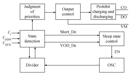
Fig. 1.
The single lithium-ion battery protection circuit
SEMICONDUCTOR INTEGRATED CIRCUITS
Jinguang Jiang1, 2, and Sen Li3
Corresponding author: Jiang Jinguang, Email:jgjiang09@aliyun.com
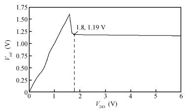
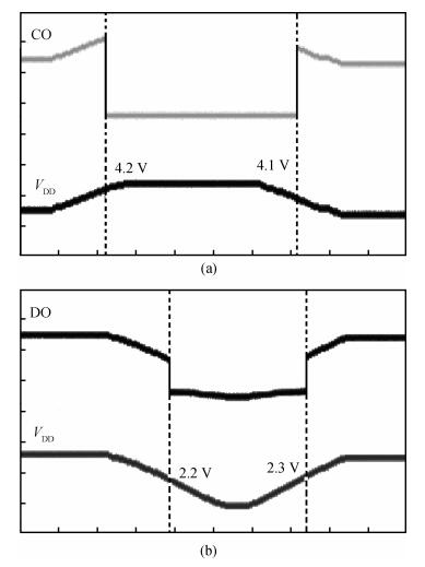
Abstract: A single lithium-ion battery protection circuit with high reliability and low power consumption is proposed. The protection circuit has high reliability because the voltage and current of the battery are controlled in a safe range. The protection circuit can immediately activate a protective function when the voltage and current of the battery are beyond the safe range. In order to reduce the circuit's power consumption, a sleep state control circuit is developed. Additionally, the output frequency of the ring oscillation can be adjusted continuously and precisely by the charging capacitors and the constant-current source. The proposed protection circuit is fabricated in a 0.5 μm mixed-signal CMOS process. The measured reference voltage is 1.19 V, the overvoltage is 4.2 V and the undervoltage is 2.2 V. The total power is about 9 μW.
Keywords: lithium-ion battery, OV, UV, reference voltage, overcurrent (OC), short circuit (SC)
| [1] |
Zhang H, Sun Y, Ding S, et al. Full-digital lithium battery protection and charging circuit based on DSP. 27th Chinese Control Conference, 2008:265
|
| [2] |
Hsieh Y C, Wu J L, Kuo Q Y. A Li-ion battery string protection system. International Conference on Applied Electronics, 2011:1 http://ieeexplore.ieee.org/document/6049095/authors
|
| [3] |
Chan C C. The state of the art of electric, hybrid, and fuel cell vehicles. Proc IEEE, 2007, 95:704 doi: 10.1109/JPROC.2007.892489
|
| [4] |
Lee Y S, Wang W Y, Kuo T Y. Soft computing for battery state-of-charge (BSOC) estimation in battery string circuit. IEEE Trans Industrial Electron, 2008, 55:229 doi: 10.1109/TIE.2007.896496
|
| [5] |
Moore S W, Schneider P J. A review of cell equalization methods for lithium ion and lithium polymer battery circuits. Adv Hybrid Vehicle Powertrains, 2001:68 http://papers.sae.org/2001-01-0959/
|
| [6] |
Lukic S M, Bansal R C, Rodriguez F, et al. Energy storage circuits for automotive applications. IEEE Trans Ind Electron, 2008, 55:2258 doi: 10.1109/TIE.2008.918390
|
| [7] |
Kuhn B T, Pitel G E, Krein P T. Electrical properties and equalization of lithium-ion cells in automotive applications. IEEE Vehicle power and Propulsion Conference, 2005:55
|
| [8] |
Kim C H, Kim M Y, Kim Y D, et al. A modularized charge equalizer using battery monitoring IC for series connected Li-ion battery strings in an electric vehicle. Power Electronics and ECCE Asia, 2011:304 http://ieeexplore.ieee.org/abstract/document/5944609/
|
| [9] |
Ye Zhihao, Wu Xiaobo, Sun Yueming, et al. A universal protection controller for Li-ion battery charger. Power and Energy Engineering Conference, 2010:1 http://ieeexplore.ieee.org/document/5448749/authors
|
| [10] |
Affanni A, Bellini A, Franceschini G, et al. Battery choice and management for new-generation electric vehicles. IEEE Trans Industrial Electron, 2005, 52:1343 http://porto.polito.it/1503806/
|
| [11] |
Sawada M, Arai H, Takahashi H, et al. Second-generation one chip Li-ion battery protection IC with an asymmetric bidirectional trench lateral power MOSFET. 22nd International Symposium on Power Semiconductor Devices & IC's, 2010:281 http://ieeexplore.ieee.org/document/5543976/?arnumber=5543976&punumber%3D5528430
|
| [12] |
Puviwatnangkurn W, Tanboonjit B, Fuengwarodsakul N H. Overcurrent protection scheme of BMS for Li-ion battery used in electric bicycles. 10th International Conference on Electrical Engineering, Computer, Telecommunications and Information Technology, 2013:1
|
| [13] |
Matsunaga S, Sawada M, Sugimoto M, et al. Low parasitic current 'half on' operation of battery protection IC. 19th International Symposium on Power Semiconductor Devices and IC's, 2007:49
|
| [14] |
Chen Min, Liu Jianchao. The design of a Li-ion battery protection IC for S ingle cell pack. Microprocessors, 2008, (1):22
|
| [15] |
Zou Xuecheng, Li Yuchao, Jiang Juan, et al. Improvement of the protection circuit for single cell pack Li-ion battery. J Huazhong University of Sci & Tech, 2007, 35:54
|
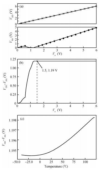
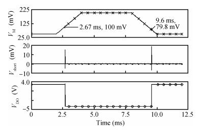
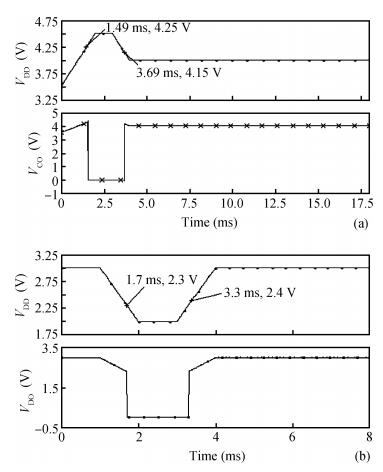
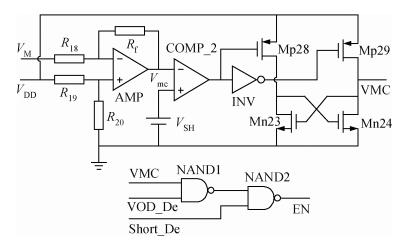
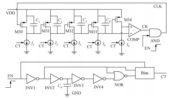
Table 1. Eight kinds of EN signal

|
Table 2. The protection criteria and the working conditions

|
Table 3. Comparison between this work and related lithium-ion battery protection circuits

|
| [1] |
Zhang H, Sun Y, Ding S, et al. Full-digital lithium battery protection and charging circuit based on DSP. 27th Chinese Control Conference, 2008:265
|
| [2] |
Hsieh Y C, Wu J L, Kuo Q Y. A Li-ion battery string protection system. International Conference on Applied Electronics, 2011:1 http://ieeexplore.ieee.org/document/6049095/authors
|
| [3] |
Chan C C. The state of the art of electric, hybrid, and fuel cell vehicles. Proc IEEE, 2007, 95:704 doi: 10.1109/JPROC.2007.892489
|
| [4] |
Lee Y S, Wang W Y, Kuo T Y. Soft computing for battery state-of-charge (BSOC) estimation in battery string circuit. IEEE Trans Industrial Electron, 2008, 55:229 doi: 10.1109/TIE.2007.896496
|
| [5] |
Moore S W, Schneider P J. A review of cell equalization methods for lithium ion and lithium polymer battery circuits. Adv Hybrid Vehicle Powertrains, 2001:68 http://papers.sae.org/2001-01-0959/
|
| [6] |
Lukic S M, Bansal R C, Rodriguez F, et al. Energy storage circuits for automotive applications. IEEE Trans Ind Electron, 2008, 55:2258 doi: 10.1109/TIE.2008.918390
|
| [7] |
Kuhn B T, Pitel G E, Krein P T. Electrical properties and equalization of lithium-ion cells in automotive applications. IEEE Vehicle power and Propulsion Conference, 2005:55
|
| [8] |
Kim C H, Kim M Y, Kim Y D, et al. A modularized charge equalizer using battery monitoring IC for series connected Li-ion battery strings in an electric vehicle. Power Electronics and ECCE Asia, 2011:304 http://ieeexplore.ieee.org/abstract/document/5944609/
|
| [9] |
Ye Zhihao, Wu Xiaobo, Sun Yueming, et al. A universal protection controller for Li-ion battery charger. Power and Energy Engineering Conference, 2010:1 http://ieeexplore.ieee.org/document/5448749/authors
|
| [10] |
Affanni A, Bellini A, Franceschini G, et al. Battery choice and management for new-generation electric vehicles. IEEE Trans Industrial Electron, 2005, 52:1343 http://porto.polito.it/1503806/
|
| [11] |
Sawada M, Arai H, Takahashi H, et al. Second-generation one chip Li-ion battery protection IC with an asymmetric bidirectional trench lateral power MOSFET. 22nd International Symposium on Power Semiconductor Devices & IC's, 2010:281 http://ieeexplore.ieee.org/document/5543976/?arnumber=5543976&punumber%3D5528430
|
| [12] |
Puviwatnangkurn W, Tanboonjit B, Fuengwarodsakul N H. Overcurrent protection scheme of BMS for Li-ion battery used in electric bicycles. 10th International Conference on Electrical Engineering, Computer, Telecommunications and Information Technology, 2013:1
|
| [13] |
Matsunaga S, Sawada M, Sugimoto M, et al. Low parasitic current 'half on' operation of battery protection IC. 19th International Symposium on Power Semiconductor Devices and IC's, 2007:49
|
| [14] |
Chen Min, Liu Jianchao. The design of a Li-ion battery protection IC for S ingle cell pack. Microprocessors, 2008, (1):22
|
| [15] |
Zou Xuecheng, Li Yuchao, Jiang Juan, et al. Improvement of the protection circuit for single cell pack Li-ion battery. J Huazhong University of Sci & Tech, 2007, 35:54
|


Article views: 3504 Times PDF downloads: 33 Times Cited by: 0 Times
Received: 20 April 2014 Revised: 06 June 2014 Online: Published: 01 November 2014
| Citation: |
Jinguang Jiang, Sen Li. A single lithium-ion battery protection circuit with high reliability and low power consumption[J]. Journal of Semiconductors, 2014, 35(11): 115010. doi: 10.1088/1674-4926/35/11/115010
****
J G Jiang, S Li. A single lithium-ion battery protection circuit with high reliability and low power consumption[J]. J. Semicond., 2014, 35(11): 115010. doi: 10.1088/1674-4926/35/11/115010.

|
| [1] |
Zhang H, Sun Y, Ding S, et al. Full-digital lithium battery protection and charging circuit based on DSP. 27th Chinese Control Conference, 2008:265
|
| [2] |
Hsieh Y C, Wu J L, Kuo Q Y. A Li-ion battery string protection system. International Conference on Applied Electronics, 2011:1 http://ieeexplore.ieee.org/document/6049095/authors
|
| [3] |
Chan C C. The state of the art of electric, hybrid, and fuel cell vehicles. Proc IEEE, 2007, 95:704 doi: 10.1109/JPROC.2007.892489
|
| [4] |
Lee Y S, Wang W Y, Kuo T Y. Soft computing for battery state-of-charge (BSOC) estimation in battery string circuit. IEEE Trans Industrial Electron, 2008, 55:229 doi: 10.1109/TIE.2007.896496
|
| [5] |
Moore S W, Schneider P J. A review of cell equalization methods for lithium ion and lithium polymer battery circuits. Adv Hybrid Vehicle Powertrains, 2001:68 http://papers.sae.org/2001-01-0959/
|
| [6] |
Lukic S M, Bansal R C, Rodriguez F, et al. Energy storage circuits for automotive applications. IEEE Trans Ind Electron, 2008, 55:2258 doi: 10.1109/TIE.2008.918390
|
| [7] |
Kuhn B T, Pitel G E, Krein P T. Electrical properties and equalization of lithium-ion cells in automotive applications. IEEE Vehicle power and Propulsion Conference, 2005:55
|
| [8] |
Kim C H, Kim M Y, Kim Y D, et al. A modularized charge equalizer using battery monitoring IC for series connected Li-ion battery strings in an electric vehicle. Power Electronics and ECCE Asia, 2011:304 http://ieeexplore.ieee.org/abstract/document/5944609/
|
| [9] |
Ye Zhihao, Wu Xiaobo, Sun Yueming, et al. A universal protection controller for Li-ion battery charger. Power and Energy Engineering Conference, 2010:1 http://ieeexplore.ieee.org/document/5448749/authors
|
| [10] |
Affanni A, Bellini A, Franceschini G, et al. Battery choice and management for new-generation electric vehicles. IEEE Trans Industrial Electron, 2005, 52:1343 http://porto.polito.it/1503806/
|
| [11] |
Sawada M, Arai H, Takahashi H, et al. Second-generation one chip Li-ion battery protection IC with an asymmetric bidirectional trench lateral power MOSFET. 22nd International Symposium on Power Semiconductor Devices & IC's, 2010:281 http://ieeexplore.ieee.org/document/5543976/?arnumber=5543976&punumber%3D5528430
|
| [12] |
Puviwatnangkurn W, Tanboonjit B, Fuengwarodsakul N H. Overcurrent protection scheme of BMS for Li-ion battery used in electric bicycles. 10th International Conference on Electrical Engineering, Computer, Telecommunications and Information Technology, 2013:1
|
| [13] |
Matsunaga S, Sawada M, Sugimoto M, et al. Low parasitic current 'half on' operation of battery protection IC. 19th International Symposium on Power Semiconductor Devices and IC's, 2007:49
|
| [14] |
Chen Min, Liu Jianchao. The design of a Li-ion battery protection IC for S ingle cell pack. Microprocessors, 2008, (1):22
|
| [15] |
Zou Xuecheng, Li Yuchao, Jiang Juan, et al. Improvement of the protection circuit for single cell pack Li-ion battery. J Huazhong University of Sci & Tech, 2007, 35:54
|

 WeChat ID
Journal of Semiconductors © 2017 All Rights Reserved 京ICP备05085259号-2

 DownLoad: