Processing math: 100%
J. Semicond. > 2014, Volume 35 > Issue 12 > 124005

SEMICONDUCTOR DEVICES

A gate current 1/f noise model for GaN/AlGaN HEMTs

Yu'an Liu and Yiqi Zhuang

+ Author Affiliations

 Corresponding author: Liu Yu'an, Email:danu0012004@163.com

DOI: 10.1088/1674-4926/35/12/124005

PDF

Abstract: This work presents a theoretical and experimental study on the gate current 1/f noise in AlGaN/GaN HEMTs. Based on the carrier number fluctuation in the two-dimensional electron gas channel of AlGaN/GaN HEMTs, a gate current 1/f noise model containing a trap-assisted tunneling current and a space charge limited current is built. The simulation results are in good agreement with the experiment. Experiments show that, if Vg < Vx (critical gate voltage of dielectric relaxation), gate current 1/f noise comes from the superimposition of trap-assisted tunneling RTS (random telegraph noise), while Vg > Vx, gate current 1/f noise comes from not only the trap-assisted tunneling RTS, but also the space charge limited current RTS. This indicates that the gate current 1/f noise of the GaN-based HEMTs device is sensitive to the interaction of defects and the piezoelectric relaxation. It provides a useful characterization tool for deeper information about the defects and their evolution in AlGaN/GaN HEMTs.

Key words: 1/f noisegate leakageAlGaN/GaNHEMT

The GaN/AlGaN HEMTs devices still suffer from gate leakage and reliability problems. Many groups have been investigating the gate leakage[1, 2] and reliability issues[3, 4], however, the physical basis of the gate leakage and the reliability problem has not been fully understood. The means of the electrical parameters characterize the gate leakage reliability, which has limited sensitivity. Low frequency noise (LFN) measurements are helpful for getting deeper information about the nature of the defects and their evolution before and after application of the stress[5, 6]. Although as early as 2001, Kotchetkov et al. proposed a gate voltage low frequency noise model based on mobility fluctuation[7]. Meanwhile, Han et al. reported a gate current low frequency noise model based on carrier number fluctuation, which includes thermal activation, tunneling, random walk of electrons[8]. Later, Katz et al. believed that the surface potential fluctuation is responsible to gate current low frequency noise[9]. Rao et al. found that the gate current noise spectra show up as random telegraph signal noise, and it has a weak correlation with the drain current noise[10, 11]. Marko et al. thought that gate current RTS is due to modulation of the gate current in the percolation path of the action of single defects[12]. Karboyan et al. found that a higher leakage current can generate numerous traps, leading to a change of the number of carriers[13]. Rendek and Šatka et al. studied gate current noise during the illumination and its slow relaxation to the initial value after the illumination[14, 15]. Kumar et al. studied different types of noise and their possible reasons[16]. Tartarin et al. researched gate defects in AlGaN/GaN HEMTs by low frequency noise measurements[17]. Xu et al. considered space charge limited gate current noise in AlGaN/GaN HEMTs[18]. Most research about the gate current noise is only related to the phenomenon described; a small model was established, and the existing models cannot explain the newly discovered phenomenon, such as space charge limited gate current noise. In this paper, the mechanism of the gate current 1/f noise is introduced, a gate current 1/f noise model containing trap-assisted tunneling current and space charge limited current is built, and the gate current noise model is successfully employed to explain the simulated and the measured results.

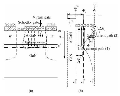
The gate current noise model will be divided into two parts, at low gate voltage, there is the trap-assisted tunneling current noise, while at high gate voltage, due to the interaction between the thermal active defect and the carriers induced by piezoelectric relaxation, resulting in a space charge limited current noise[19]. As is shown in Fig. 1, the possible leakage current paths come from the gate electrode.

Figure  1.  (a) Cross section of an AlGaN/GaN HEMT, where the virtual gate effect leads to the depletion extended, meanwhile, the interaction between the space charge and piezoelectric dipole charge will result in the gate current 1/f noise. (b) Corresponding energy band diagram of the AlGaN/GaN HEMT, where Ec is conduction band energy level of GaN. Vg is the bias on the gate relative to the source. EF1 and EF2 is Fermi level correspondence to Vg < 0 and Vg > 0, respectively. Φt is the difference in potential between the AlGaN conduction band and the traps. Φb is the Schottky barrier height, equal to the amount of energy by which the bottom of the conduction band discontinuity ΔΦc is above the Fermi energy, where the xm is the thickness of the AlGaN layer. ΔEa is the activation energy associated with the surface trap-to-trap current conduction. The two arrows denote the two gate current paths, respectively.

Studies suggest that there are two gate leakage paths[20]: (1) the electrons which come from the gate electrode may pass through the AlGaN layer to the two-dimensional electron gas (2DEG) conducting channel, it becomes the trap assisted tunneling current. (2) The electrons which come from the gate electrode may be accumulated on the side of the semiconductor surface, or it becomes a hot carrier injection to the drain by being thermally activated, generating a gate-to-drain leakage current, which is a space charge limited current. Meanwhile, it will generate RTS noise from the trap-to-trap mechanism or the conductive transition, where the space charge limited current threshold gate voltage (Vx=qn0L2/ε) is defined as the voltage when the charge transfer time ttr=L/Vd=L2/μV is equal to the medium relaxation time trelax=ρε=εqn0μ [19]. If Vg < Vx, gate leakage is the corresponding path (1). If Vg > Vx, gate leakage is the corresponding path (2).

Next, we discuss the gate current noise model. Each trap causes an RTS in the gate current with amplitude ΔI=aJG, average time in the low state (filled trap) τoff and average time in the high state (empty trap) τon. Thus the power spectral density (PSD) is given by[21],

SRTS=4(aJG)2fT(1fT)τC1+(ωτC)2,

(1)

(τC)1=(τoff)1+(τon)1.

(2)

The trap occupation probability

fT=τoff/(τoff+τon).

(3)

The RTS time constants are

1τon=1τ0T(Ex)fT,

(4)

1τoff=1τ0T(Ex)(1fT),

(5)

where τ0 is a characteristic time constant and T(Ex) is the transmission coefficient for electron tunneling between the AlGaN interface and the considered trap position at the considered trap energy.

If Vg < Vx, the gate current is based on the TSB model[22]. The current through the Schottky barrier with an arbitrary potential profile through

JG=4πqmh30T(Ex)×0[fs(Ep+Ex)fm(Ep+Ex)]dEpdEx,

(6)

where T(Ex) is the tunneling probability for Ex=h22mk2x, i.e., the energy component normal to the Schottky interface, fs and fm are Fermi-Dirac distribution functions in the semiconductor and in the metal, respectively, and Ep=h22m(k2y+k2z) i.e., the energy component parallel to the interface. T(Ex) was calculated under the Wentzel-Kramers-Brillouin (WKB) approximation as follows.

T(Ex)=exp[22mx2x1ϕ(x)Exdx].

(7)

The defect has the following exponentially decaying distribution into the depth, x, from the surface:

NT(x)=NT0exp(x/λ).

(8)

The PSD, given by all the traps, and assumed uncorrelated, can be obtained by the superimposition,

Sig=Axmax0ϕB0SRTS(x,E)NT(Ex)dEdx,

(9)

where A is the device area and E= 0 corresponds to the bottom of the conduction band EC at the substrate interface.

Sig=4a2I2GAxmax0ϕB0fT(E)[1fT(E)]τC(Ex)1+[ωτC(Ex)]2×NT(Ex)dEdx.

(10)

Since the function fT(E)[1fT(E)]kTδ(EEF), it follows that

Sig=4a2I2GkTNT(Ex)Axmax0τC(Ex)1+[ωτC(Ex)]2dx.

(11)

If Vg > Vx, the electrons that tunnel from the gate can be localized in the surface defects (most likely nitrogen vacancies) and/or dangling bonds, not only the trap assisted tunneling current, but also the space charge limited current. It can travel over multiple barriers with spacing and barrier height Ea, as shown in Fig. 1. of gate current path (2). Space charge limited current noise is superimposed by RTS noise. The time constant of the charge fluctuation can be calculated based on a hot carrier induced trap model[23], (τi)1=(τc)1+(τe)1.

The ratio τc/τe is related to the trap energy relative to the Fermi energy level, ETEF, and degeneracy factor g,

τcτe=τHτL=ge(EcETΦAlGaN+qVg)/kT,

(12)

where Ec is the conduction band energy of GaN, ΦAlGaN is the height of AlGaN barriers, and Vg is the gate voltage.

τc=1/σnˉv=τc0exp(Ea/KT),

(13)

where σ is the capture section of carriers, ˉv is the carriers average speed of thermal motion, n is the 2DEG concentration, τc0 is the inverse phonon frequency, and Ea is the activation energy associated with the surface trap-to-trap current conduction.

Then, the total expression for the gate current noise is

Sig=4a2I2GkTNT(Ex)Axmax0[τC(Ex)1+[ωτC(Ex)]2+τC0exp(Ea/kT)1+[ω/σnˉv]2]dx.

(14)

In order to validate the proposed model, we measured the gate-drain current and gate current noise in AlGaN/GaN HEMTs by using a purposely designed measurement setup.

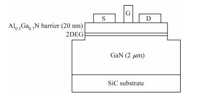
It consisted of a 200 nm GaN buffer layer and a 20 nm Al0.3Ga0.7N layer is grown on a high resistivity SiC substrate by metal organic chemical vapor deposition (MOCVD). A Schottky gate contact of Ni/Au (20 nm/20 nm) is formed by electron beam evaporation. Ohmic contacts of the Ti/Al/Ni/Au (20 nm/120 nm/55/45 nm) are created for the drain and source regions by electron beam evaporation. The transistor has a gate width of 100 μm, and a gate length of 0.6 μm. The device structure is shown in Fig. 2.

Figure  2.  Device structure and the movement of the stress produced carriers, where SGD represents the device's source drain and gate, respectively.

The difference of our experiment with Xu[19] is that they are measuring Igs-Vgs, however, the authors believe that the gate leakage current due to space limitations is mainly produced in the drain terminal, and Igd is more sensitive to its changes; therefore, we use the semiconductor parameter analyzer HP4156B to measure the electronic parameters Igd-Vgs of the device under different bases (Vgs < Vx and Vgs > Vx).

Gate current 1/f noise of all devices is measured by a noise testing and analyzing system of an electronic device based on a virtual instrument, which is developed in our lab. It includes four parts, bias circuits, low-noise preamplifier, data acquisition card and microcomputer. The source and drain of the device are grounded, it is the means Vs=Vb= 0 V. All tests are carried out in a shield room at room temperature. The device operates in the linear region in the noise measurement.

Measured Igd-Vgs curves of the end test device show predominantly a power law rather than exponential current voltage dependences, as illustrated in Fig. 3. For Vgs < 0.6 V, the Igd-Vgs slope is 1, which indicates an ohmic relationship. At the same time, the gate stack works as a capacitor to accumulate carriers inside the leakage path. This indicates that the increase in gate current is caused by merely an expansion of the leakage path due to the stress applied. The newly created conductive paths have similar trap-related transport characteristics to those which originally existed in the unstressed device. When the traps are being filled up with increasing gate voltage, a sudden increase in current is expected. When the gate bias increases until injected carriers exceed the number of electrons originally located in the conductive path, the Igd-Vgs slope increases to a value of 2 indicative of an SCLC flow. This result has the same trend as Wei's[19].

Figure  3.  Measured gate-drain current as a function of the magnitude of the gate voltage.

The gate current 1/f noise of an AlGaN/GaN HEMT device under different biases is shown in Fig. 4. There are two groups of curves corresponding to the two cases. In case 1, Vg = 0.6 V, Vx = 1.0 V, where Vg < Vx, the gate current 1/f noise complies with Eq. (11). It is superimposed by the RTS noise and background 1/f noise, where the RTS noise is induced by the trap assisted tunneling processes of deep traps (as is shown in Fig. 1, gate current path (1)). The simulation results and experimental data are shown in Fig. 4 curve 1, the gray line shows the measured data, and the black line represents the simulation result. Most of these two curves coincide. In case 2, Vg = 1.1 V, Vx = 1.0 V, where Vg > Vx, gate current 1/f noise complies with Eq. (14), where it is superimposed by RTS noise and space charge limited current noise. The former is induced by the trap assisted tunneling processes of deep traps (as is shown in Fig. 1, gate current path (1)), while the latter is induced by being piezoelectric induced surface carrier thermally activated (as is shown in Fig. 1, gate current path (2)). The simulation results and experimental data are shown in Fig. 4 curve 2, the gray line shows the measured data, and the black line represents the simulation result. Most of these two curves coincide. All these results are consistent with the result of Xu[18].

Figure  4.  The gate current 1/f noise of an AlGaN/GaN HEMTs device under different biases.

The simulation using MATLAB software, based on the multi-parameter 1/f noise model. Simulation parameters are used as follows: trap density NT = 1 × 1018 cm3, NT0 = 1.5 × 1017 cm3, the height of the AlGaN barrier Φb = 1.62 eV, capture section of carriers σ = 1.2 × 1016 cm2, activation energy Ea = 0.201 eV, channel mobility μ = 1420 cm2/(Vs), GaN permittivity ε = 10.1, conduction band discontinuity ΔΦC = 0.37 V, and channel carrier concentration n = 1 × 1013 cm3.

Gate current 1/f noise in AlGaN/GaN HEMTs is studied theoretically and experimentally. A gate current 1/f noise model containing trap-assisted tunneling current and space charge limited current is built, which is based on the fluctuations of the number of carriers in the two-dimensional electron gas (2DEG) channel of AlGaN/GaN HEMTs. Experiments show that, if Vg < Vx (critical gate voltage of dielectric relaxation), the Ig-Vg slope is 1, meanwhile, gate current 1/f noise comes from the superimposition of trap-assisted tunneling RTS (random telegraph noise). While, Vg < V, the Ig-Vg slope is suddenly increasing from 1 to 2, gate current 1/f noise comes from not only the trap-assisted tunneling RTS, but also the space charge limited current RTS. This indicates that gate current 1/f noise of the GaN-based HEMTs device is sensitive to the interaction of defects and the piezoelectric relaxation. The simulation results are in good agreement with the experimental results. It provides a useful characterization tool for deeper information about the defects and their evolution in AlGaN/GaN HEMTs.


[1]
Asgari A, Karamad M, Kalafi M. Modeling of trap-assisted tunneling in AlGaN/GaN heterostructure field effect transistors with different Al mole fractions. Superlattices and Microstructures, 2006, 40:603 doi: 10.1016/j.spmi.2006.07.023
[2]
Hasegawa H, Inagaki T, Ootomo S, et al. Mechanisms of current collapse and gate leakage currents in AlGaN/GaN heterostructure field effect transistors. J Vac Sci Technol B-Microelectronics and Nanometer Structures, 2003, 21(4):1844 doi: 10.1116/1.1589520
[3]
Del Alamo J A, Joh J. GaN HEMT reliability. Microelectron Reliab, 2009, 49:1200 doi: 10.1016/j.microrel.2009.07.003
[4]
Tartarin J G. Diagnostic tools for accurate reliability investigations of GaN devices. 21st International Conference on Noise and Fluctuations, 2011:452
[5]
Rao H, Bosman G. Study of RF reliability of GaN HEMTs using low-frequency noise spectroscopy. IEEE Trans Device Mater Reliab, 2012, 12(1):31 doi: 10.1109/TDMR.2011.2173497
[6]
Marko P, Meneghini M, Bychikhin S, et al. Noise and electroluminescence analysis of stress-induced percolation paths in AlGaN/GaN high electron mobility transistors. Microelectron Reliab, 2012, 52:2194 doi: 10.1016/j.microrel.2012.06.030
[7]
Kotchetkov D, Balandin A A. Carrier-density fluctuation noise and the interface trap density in GaN/AlGaN HFETs. Mat Res Soc Symp Proc, 2001:680
[8]
Han I K, Lee J I. Low frequency noise in HEMT structure. Journal of the Korean Physical Society, 2001, 39:S322
[9]
Katz O, Bahir G, Salzman J. Low-frequency 1/f noise and persistent transients in AlGaN-GaN HFETs. IEEE Electron Device Lett, 2005, 26(6):345 doi: 10.1109/LED.2005.848092
[10]
Rao H, Bosman G. Simultaneous low-frequency noise characterization of gate and drain currents in AlGaN/GaN high electron mobility transistors. J Appl Phys, 2009, 106:103712 doi: 10.1063/1.3259437
[11]
Rao H, Bosman G. Device reliability study of AlGaN/GaN high electron mobility transistors under high gate and channel electric fields via low frequency noise spectroscopy. Microelectron Reliab, 2010, 50:1528 doi: 10.1016/j.microrel.2010.07.073
[12]
Marko P, Alexewicz A, Hilt O, et al. Random telegraph signal noise in gate current of unstressed and reverse bias-stressed AlGaN/GaN high electron mobility transistors. Appl Phys Lett, 2012, 100:143507 doi: 10.1063/1.3701164
[13]
Karboyan S, Tartarin J G, Labat N, et al. Gate and drain low frequency noise of ALGAN/GAN HEMTs featuring high and low gate leakage currents. IEEE 22nd International Conference on Noise and Fluctuations (ICNF), 2013:1
[14]
Rendek K, Satka A, Donoval D. Measurement set-up for low-frequency noise characterization of GaN HEMT transistors. IEEE 22nd International Conference on Radioelektronika, 2012:1
[15]
Satka A, Rendek K, Priesol J. Relaxation of low-frequency noise in AlGaN/GaN HEMTs. IEEE Ninth International Conference on Advanced Semiconductor Devices & Microsystems (ASDAM), Smolenice, Slovakia, 2012:19
[16]
Kumar N, Kumar P, Kumar A. AlGaN/GaN HFET:operating principle and noise performance. International Journal of Advanced Trends in Computer Science and Engineering, 2013, 2(4):86
[17]
Tartarin J G, Karboyan S, Carisetti D, et al. Gate defects in AlGaN/GaN HEMTs revealed by low frequency noise measurements. IEEE 22nd International Conference on Noise and Fluctuations (ICNF), 2013
[18]
Xu W, Bosman G. Space charge limited current noise in AlGaN/GaN HEMTs. IEEE 22nd International Conference on Noise and Fluctuations (ICNF), 2013
[19]
Xu W, Rao H, Bosman G. Evidence of space charge limited flow in the gate current of AlGaN/GaN high electron mobility transistors. Appl Phys Lett, 2012, 100:223504 doi: 10.1063/1.4724207
[20]
Sudharsanan S, Karmalkar S. Modeling of the reverse gate leakage in AlGaN/GaN high electron mobility transistors. J Appl Phys, 2010, 107:064501 doi: 10.1063/1.3340826
[21]
Crupi F, Magnone P, Simoen E, et al. The role of the interfaces in the 1/f noise of MOSFETs with high-k gate stacks. ECS Trans, 2009, 19(2):87
[22]
Hasegawa H, Akazawa M. Current transport, Fermi level pinning, and transient behavior of group-Ⅲ nitride Schottky barriers. Journal of the Korean Physical Society, 2009, 55(3):1167
[23]
Vitusevich S A, Danylyuk S V, Kurakin A M. Origin of noise in AlGaN/GaN heterostructures in the range of 10-100 MHz. J Appl Phys, 2006, 99:0737061
Fig. 1.  (a) Cross section of an AlGaN/GaN HEMT, where the virtual gate effect leads to the depletion extended, meanwhile, the interaction between the space charge and piezoelectric dipole charge will result in the gate current 1/f noise. (b) Corresponding energy band diagram of the AlGaN/GaN HEMT, where Ec is conduction band energy level of GaN. Vg is the bias on the gate relative to the source. EF1 and EF2 is Fermi level correspondence to Vg < 0 and Vg > 0, respectively. Φt is the difference in potential between the AlGaN conduction band and the traps. Φb is the Schottky barrier height, equal to the amount of energy by which the bottom of the conduction band discontinuity ΔΦc is above the Fermi energy, where the xm is the thickness of the AlGaN layer. ΔEa is the activation energy associated with the surface trap-to-trap current conduction. The two arrows denote the two gate current paths, respectively.

Fig. 2.  Device structure and the movement of the stress produced carriers, where SGD represents the device's source drain and gate, respectively.

Fig. 3.  Measured gate-drain current as a function of the magnitude of the gate voltage.

Fig. 4.  The gate current 1/f noise of an AlGaN/GaN HEMTs device under different biases.

[1]
Asgari A, Karamad M, Kalafi M. Modeling of trap-assisted tunneling in AlGaN/GaN heterostructure field effect transistors with different Al mole fractions. Superlattices and Microstructures, 2006, 40:603 doi: 10.1016/j.spmi.2006.07.023
[2]
Hasegawa H, Inagaki T, Ootomo S, et al. Mechanisms of current collapse and gate leakage currents in AlGaN/GaN heterostructure field effect transistors. J Vac Sci Technol B-Microelectronics and Nanometer Structures, 2003, 21(4):1844 doi: 10.1116/1.1589520
[3]
Del Alamo J A, Joh J. GaN HEMT reliability. Microelectron Reliab, 2009, 49:1200 doi: 10.1016/j.microrel.2009.07.003
[4]
Tartarin J G. Diagnostic tools for accurate reliability investigations of GaN devices. 21st International Conference on Noise and Fluctuations, 2011:452
[5]
Rao H, Bosman G. Study of RF reliability of GaN HEMTs using low-frequency noise spectroscopy. IEEE Trans Device Mater Reliab, 2012, 12(1):31 doi: 10.1109/TDMR.2011.2173497
[6]
Marko P, Meneghini M, Bychikhin S, et al. Noise and electroluminescence analysis of stress-induced percolation paths in AlGaN/GaN high electron mobility transistors. Microelectron Reliab, 2012, 52:2194 doi: 10.1016/j.microrel.2012.06.030
[7]
Kotchetkov D, Balandin A A. Carrier-density fluctuation noise and the interface trap density in GaN/AlGaN HFETs. Mat Res Soc Symp Proc, 2001:680
[8]
Han I K, Lee J I. Low frequency noise in HEMT structure. Journal of the Korean Physical Society, 2001, 39:S322
[9]
Katz O, Bahir G, Salzman J. Low-frequency 1/f noise and persistent transients in AlGaN-GaN HFETs. IEEE Electron Device Lett, 2005, 26(6):345 doi: 10.1109/LED.2005.848092
[10]
Rao H, Bosman G. Simultaneous low-frequency noise characterization of gate and drain currents in AlGaN/GaN high electron mobility transistors. J Appl Phys, 2009, 106:103712 doi: 10.1063/1.3259437
[11]
Rao H, Bosman G. Device reliability study of AlGaN/GaN high electron mobility transistors under high gate and channel electric fields via low frequency noise spectroscopy. Microelectron Reliab, 2010, 50:1528 doi: 10.1016/j.microrel.2010.07.073
[12]
Marko P, Alexewicz A, Hilt O, et al. Random telegraph signal noise in gate current of unstressed and reverse bias-stressed AlGaN/GaN high electron mobility transistors. Appl Phys Lett, 2012, 100:143507 doi: 10.1063/1.3701164
[13]
Karboyan S, Tartarin J G, Labat N, et al. Gate and drain low frequency noise of ALGAN/GAN HEMTs featuring high and low gate leakage currents. IEEE 22nd International Conference on Noise and Fluctuations (ICNF), 2013:1
[14]
Rendek K, Satka A, Donoval D. Measurement set-up for low-frequency noise characterization of GaN HEMT transistors. IEEE 22nd International Conference on Radioelektronika, 2012:1
[15]
Satka A, Rendek K, Priesol J. Relaxation of low-frequency noise in AlGaN/GaN HEMTs. IEEE Ninth International Conference on Advanced Semiconductor Devices & Microsystems (ASDAM), Smolenice, Slovakia, 2012:19
[16]
Kumar N, Kumar P, Kumar A. AlGaN/GaN HFET:operating principle and noise performance. International Journal of Advanced Trends in Computer Science and Engineering, 2013, 2(4):86
[17]
Tartarin J G, Karboyan S, Carisetti D, et al. Gate defects in AlGaN/GaN HEMTs revealed by low frequency noise measurements. IEEE 22nd International Conference on Noise and Fluctuations (ICNF), 2013
[18]
Xu W, Bosman G. Space charge limited current noise in AlGaN/GaN HEMTs. IEEE 22nd International Conference on Noise and Fluctuations (ICNF), 2013
[19]
Xu W, Rao H, Bosman G. Evidence of space charge limited flow in the gate current of AlGaN/GaN high electron mobility transistors. Appl Phys Lett, 2012, 100:223504 doi: 10.1063/1.4724207
[20]
Sudharsanan S, Karmalkar S. Modeling of the reverse gate leakage in AlGaN/GaN high electron mobility transistors. J Appl Phys, 2010, 107:064501 doi: 10.1063/1.3340826
[21]
Crupi F, Magnone P, Simoen E, et al. The role of the interfaces in the 1/f noise of MOSFETs with high-k gate stacks. ECS Trans, 2009, 19(2):87
[22]
Hasegawa H, Akazawa M. Current transport, Fermi level pinning, and transient behavior of group-Ⅲ nitride Schottky barriers. Journal of the Korean Physical Society, 2009, 55(3):1167
[23]
Vitusevich S A, Danylyuk S V, Kurakin A M. Origin of noise in AlGaN/GaN heterostructures in the range of 10-100 MHz. J Appl Phys, 2006, 99:0737061
1

Monolithically integrated enhancement/depletion-mode AlGaN/GaN HEMT D flip-flop using fluorine plasma treatment

Xie Yuanbin, Quan Si, Ma Xiaohua, Zhang Jincheng, Li Qingmin, et al.

Journal of Semiconductors, 2011, 32(6): 065001. doi: 10.1088/1674-4926/32/6/065001

2

Fabrication of a 120 nm gate-length lattice-matched InGaAs/InAlAsInP-based HEMT

Huang Jie, Guo Tianyi, Zhang Haiying, Xu Jingbo, Fu Xiaojun, et al.

Journal of Semiconductors, 2010, 31(9): 094008. doi: 10.1088/1674-4926/31/9/094008

3

120-nm gate-length In0.7Ga0.3As/In0.52Al0.48As InP-based HEMT

Huang Jie, Guo Tianyi, Zhang Haiying, Xu Jingbo, Fu Xiaojun, et al.

Journal of Semiconductors, 2010, 31(7): 074008. doi: 10.1088/1674-4926/31/7/074008

4

A High Performance AlGaN/GaN HEMT with a New Method for T-Gate Layout Design

Chen Zhigang, Zhang Yang, Luo Weijun, Zhang Renping, Yang Fuhua, et al.

Journal of Semiconductors, 2008, 29(9): 1654-1656.

5

14W X-Band AlGaN/GaN HEMT Power MMICs

Chen Tangsheng, Zhang Bin, Ren Chunjiang, Jiao Gang, Zheng Weibin, et al.

Journal of Semiconductors, 2008, 29(6): 1027-1030.

6

Development and Characteristic Analysis of MOS AlGaN/GaN HEMTs

Wang Chong, Yue Yuanzheng, Ma Xiaohua, Hao Yue, Feng Qian, et al.

Journal of Semiconductors, 2008, 29(8): 1557-1560.

7

Effects of NF3 Plasma Treatment Prior to SiN Passivation on the Characteristics of AlGaN/GaN HEMTs

Ren Chunjiang, Chen Tangsheng, Jiao Gang, Chen Gang, Xue Fangshi, et al.

Journal of Semiconductors, 2008, 29(12): 2385-2388.

8

An Enhancement-Mode AlGaN/GaN HEMT with Recessed-Gate

Wang Chong, Zhang Jinfeng, Quan Si, Hao Yue, Zhang Jincheng, et al.

Journal of Semiconductors, 2008, 29(9): 1682-1685.

9

DC Characteristics of AlGaN/GaN HEMTs with a Field Plate Gate

Wei Ke, Liu Xinyu, He Zhijing, Wu Dexin

Journal of Semiconductors, 2008, 29(3): 554-558.

10

Effect of Plasma Dry Etching on Gate Leakage of Recessed AlGaN/GaN HEMTs

Li Chengzhan, Pang Lei, Liu Xinyu, Huang Jun, Liu Jian, et al.

Chinese Journal of Semiconductors , 2007, 28(11): 1777-1781.

11

Characteristic of the Recessed-Gate AIGaN/GaN HEMT with a Field Plate

Chen Chen, Chen Tangsheng, Ren Chunjiang, Xue Fangshi

Chinese Journal of Semiconductors , 2007, 28(S1): 407-410.

12

GaN MOS-HEMT Using Ultrathin Al2O3 Dielectric with fmax of 30.8GHz

Hao Yue, Yue Yuanzheng, Feng Qian, Zhang Jincheng, Ma Xiaohua, et al.

Chinese Journal of Semiconductors , 2007, 28(11): 1674-1678.

13

Output Power of an AlGaN/GaN HFET on Sapphire Substrate

Zhang Zhiguo, Yang Ruixia, Li Li, Feng Zhen, Wang Yong, et al.

Chinese Journal of Semiconductors , 2006, 27(7): 1255-1258.

14

0.25μm Gate-Length AlGaN/GaN Power HEMTs on Sapphire with fT of 77GHz

Zheng Yingkui, Liu Guoguo, He Zhijing, Liu Xinyu, Wu Dexin, et al.

Chinese Journal of Semiconductors , 2006, 27(6): 963-965.

15

MOCVD-Grown AlGaN/AlN/GaN HEMT Structure with High Mobility GaN Thin Layer as Channel on SiC

Wang Xiaoliang, Hu Guoxin, Ma Zhiyong, Xiao Hongling, Wang Cuimei, et al.

Chinese Journal of Semiconductors , 2006, 27(9): 1521-1525.

16

Degradation Under High-Field Stress and Effects of UV Irradiation on AlGaN/GaN HEMTs

Wang Chong, Zhang Jincheng, Hao Yue, Yang Yan

Chinese Journal of Semiconductors , 2006, 27(8): 1436-1440.

17

Fabrication of a High-Performance 1mm AlGaN/GaN HEMT on SiC Substrate

Luo Weijun, Chen Xiaojuan, Li Chengzhan, Liu Xinyu, He Zhijing, et al.

Chinese Journal of Semiconductors , 2006, 27(11): 1981-1983.

18

Investigation of Undoped AlGaN/GaN Microwave Power HEMT

Zeng Qingming, Li Xianjie, Zhou Zhou, Wang Yong, Wang Xiaoliang, et al.

Chinese Journal of Semiconductors , 2005, 26(S1): 151-154.

19

Effect of an AlN Spacer Layer on AlGaN/GaN HEMTs

Zhang Jincheng, Wang Chong, Yang Yan, Zhang, Zhang Jinfeng, et al.

Chinese Journal of Semiconductors , 2005, 26(12): 2396-2400.

20

AlGaN/GaN High Electron Mobility Transistors on Sapphires with fmax of 100GHz

Li Xianjie, Zeng Qingming, Zhou Zhou, Liu Yugui, Qiao Shuyun, et al.

Chinese Journal of Semiconductors , 2005, 26(11): 2049-2052.

  • Search

    Advanced Search >>

    GET CITATION

    Yu'an Liu, Yiqi Zhuang. A gate current 1/f noise model for GaN/AlGaN HEMTs[J]. Journal of Semiconductors, 2014, 35(12): 124005. doi: 10.1088/1674-4926/35/12/124005
    Y A Liu, Y Q Zhuang. A gate current 1/f noise model for GaN/AlGaN HEMTs[J]. J. Semicond., 2014, 35(12): 124005. doi:  10.1088/1674-4926/35/12/124005.
    shu

    Export: BibTex EndNote

    Article Metrics

    Article views: 2389 Times PDF downloads: 36 Times Cited by: 0 Times

    History

    Received: 21 May 2014 Revised: 14 July 2014 Online: Published: 01 December 2014

    Catalog

      Email This Article

      User name:
      Email:*请输入正确邮箱
      Code:*验证码错误
      Yu'an Liu, Yiqi Zhuang. A gate current 1/f noise model for GaN/AlGaN HEMTs[J]. Journal of Semiconductors, 2014, 35(12): 124005. doi: 10.1088/1674-4926/35/12/124005 ****Y A Liu, Y Q Zhuang. A gate current 1/f noise model for GaN/AlGaN HEMTs[J]. J. Semicond., 2014, 35(12): 124005. doi:  10.1088/1674-4926/35/12/124005.
      Citation:
      Yu'an Liu, Yiqi Zhuang. A gate current 1/f noise model for GaN/AlGaN HEMTs[J]. Journal of Semiconductors, 2014, 35(12): 124005. doi: 10.1088/1674-4926/35/12/124005 ****
      Y A Liu, Y Q Zhuang. A gate current 1/f noise model for GaN/AlGaN HEMTs[J]. J. Semicond., 2014, 35(12): 124005. doi:  10.1088/1674-4926/35/12/124005.

      A gate current 1/f noise model for GaN/AlGaN HEMTs

      DOI: 10.1088/1674-4926/35/12/124005
      More Information
      • Corresponding author: Liu Yu'an, Email:danu0012004@163.com
      • Received Date: 2014-05-21
      • Revised Date: 2014-07-14
      • Published Date: 2014-12-01

      Catalog

        /

        DownLoad:  Full-Size Img  PowerPoint
        Return
        Return