


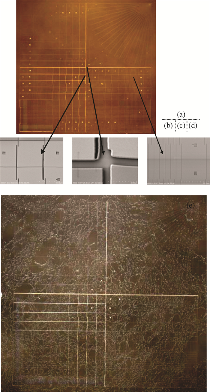
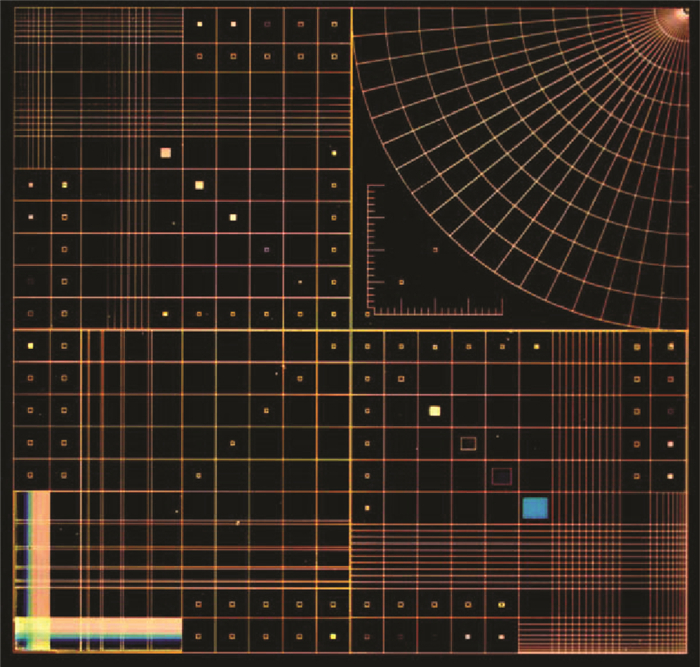
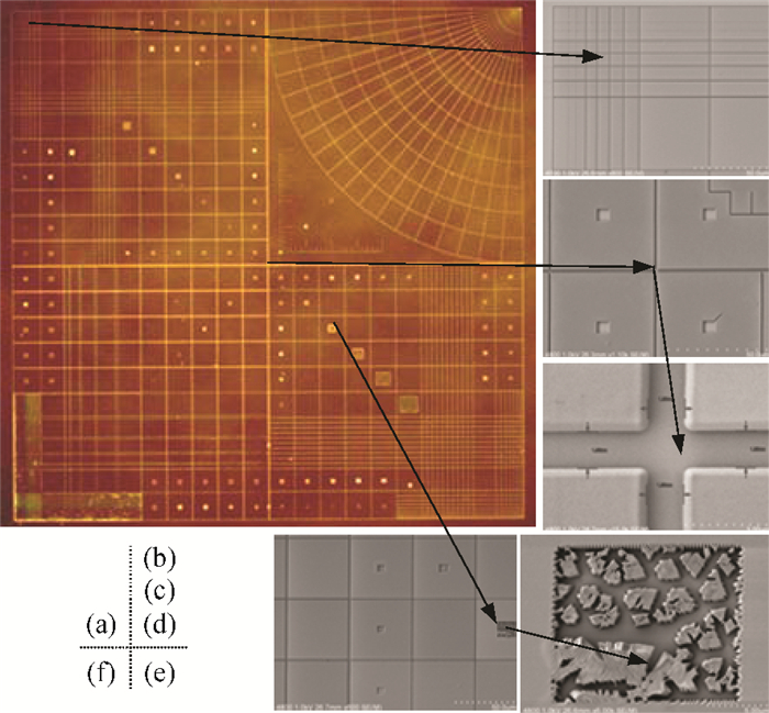
Fig. 1.
Discharge phenomenon and lines distortion of photoresist caused by the charging effect in high energy electron beam lithography on insulating substrate
SEMICONDUCTOR TECHNOLOGY
Mingyan Yu1, 2, , Shirui Zhao2, Yupeng Jing2, Yunbo Shi1 and Baoqin Chen2
Corresponding author: Yu Mingyan, Email:yumingyan@ime.ac.cn
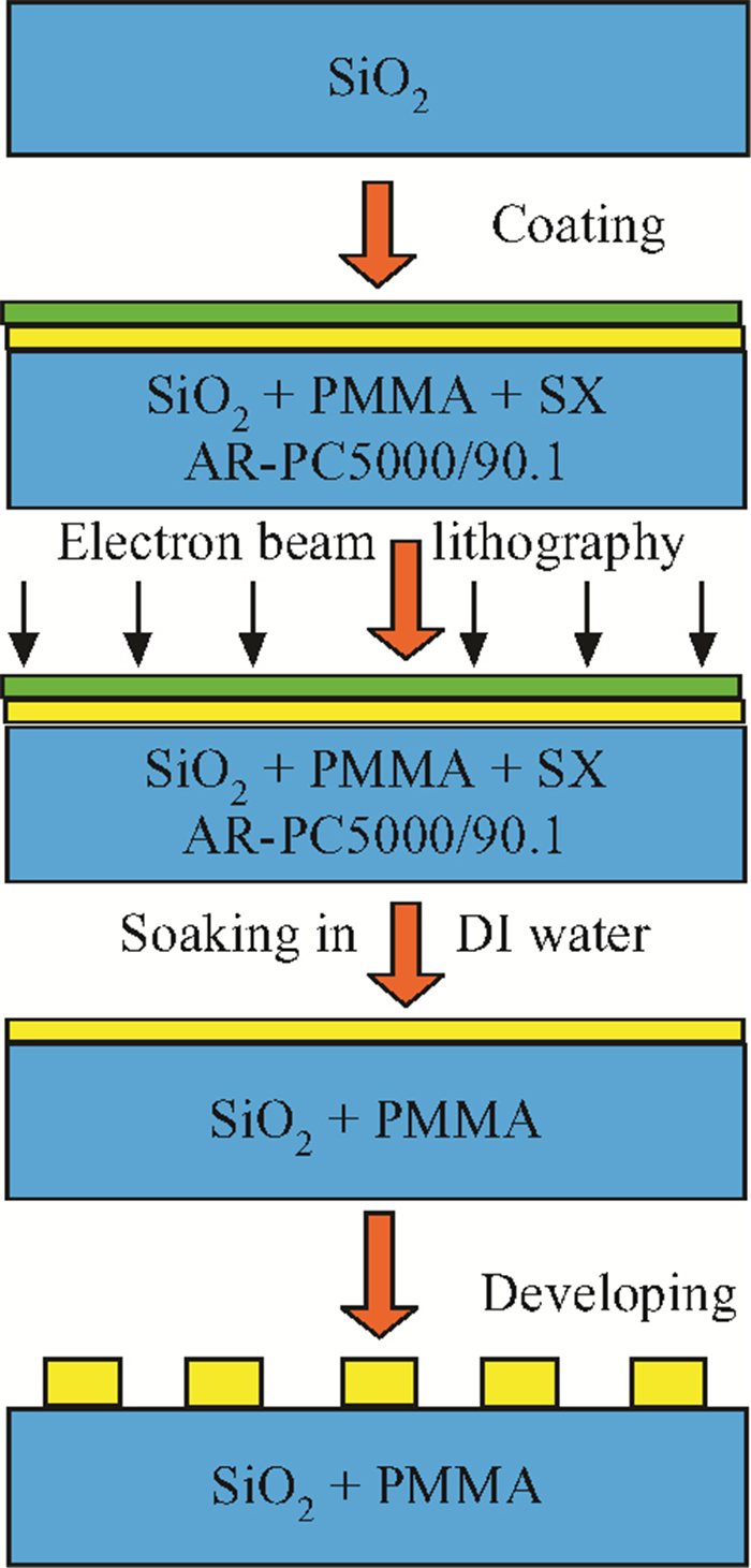
Abstract: Pattern distortions caused by the charging effect should be reduced while using the electron beam lithography process on an insulating substrate. We have developed a novel process by using the SX AR-PC 5000/90.1 solution as a spin-coated conductive layer, to help to fabricate nanoscale patterns of poly-methyl-methacrylate polymer resist on glass for phased array device application. This method can restrain the influence of the charging effect on the insulating substrate effectively. Experimental results show that the novel process can solve the problems of the distortion of resist patterns and electron beam main field stitching error, thus ensuring the accuracy of the stitching and overlay of the electron beam lithography system. The main characteristic of the novel process is that it is compatible to the multi-layer semiconductor process inside a clean room, and is a green process, quite simple, fast, and low cost. It can also provide a broad scope in the device development on insulating the substrate, such as high density biochips, flexible electronics and liquid crystal display screens.
Keywords: charging effect, pattern distortions, electron beam lithography
| [1] |
Duan H, Winston D, Yang J K W, et al. Sub-10-nm half-pitch electron-beam lithography by using poly (methyl methacrylate) as a negative resist. J Vac Sci Technol B, 2010, 28(6):C6C58 doi: 10.1116/1.3501353
|
| [2] |
Grigorescu A E, Hagen C W. Resists for sub-20-nm electron beam lithography with a focus on HSQ:state of the art. Nanotechnology, 2009, 20(29):292001 doi: 10.1088/0957-4484/20/29/292001
|
| [3] |
Cord B, Yang J, Duan H, et al. Limiting factors in sub-10 nm scanning-electron-beam lithography. J Vac Sci Technol B, 2009, 27:2616 doi: 10.1116/1.3253603
|
| [4] |
Ma S, Con C, Yavuz M, et al. Polystyrene negative resist for high-resolution electron beam lithography. Nanoscale Research Letters, 2011, 6(1):1 doi: 10.1186/1556-276X-6-446
|
| [5] |
Ren Liming, Wang Wenping, Chen Baoqin, et al. Microfabrication of nano-scale feature lines. Journal of Semiconductors, 2004, 25(12):1722 http://www.jos.ac.cn/bdtxbcn/ch/reader/view_abstract.aspx?flag=1&file_no=08032601&journal_id=bdtxbcn
|
| [6] |
Xie C Q, Zhu X L, Li H L, et al. Fabrication of X-ray diffractive optical elements for laser fusion applications. Opt Eng, 2013, 52(3):033402 doi: 10.1117/1.OE.52.3.033402
|
| [7] |
Wilson G, Evans A, Dennison J R. Electron energy dependent charging effects of multilayered dielectric materials. Bulletin of the American Physical Society, 2011:56 http://adsabs.harvard.edu/abs/2013ITPS...41.3536W
|
| [8] |
Murakawa S, McVittie J P. Mechanism of surface charging effects on etching profile defects. Jpn J Appl Phys, 1994, 33(part 1):2184 doi: 10.1143/JJAP.33.2184
|
| [9] |
Fakhfakh S, Jbara O, Fakhfakh Z. Charge transport and behavior analysis with electron irradiated (PMMA). IEEE Conference on Electrical Insulation and Dielectric Phenomena, 2009:441
|
| [10] |
Joo J, Chow B Y, Jacobson J M. Nanoscale patterning on insulating substrates by critical energy electron beam lithography. Nano Lett, 2006, 6(9):2021 doi: 10.1021/nl061211q
|
| [11] |
Satyalakshmi K M, Olkhovets A, Metzler M G, et al. Charge induced pattern distortion in low energy electron beam lithography. J Vac Sci Technol B, 2000, 18(6):3122 doi: 10.1116/1.1321755
|
| [12] |
Liu J, Li Q, Ren M, et al. Graphene as discharge layer for electron beam lithography on insulating substrate. Appl Phys Lett, 2013, 103(113107):1 http://adsabs.harvard.edu/abs/2013ApPhL.103k3107L
|
| [13] |
Bailey T C, Resnick D J, Mancini D, et al. Template fabrication schemes for step and flash imprint lithography. Microelectron Eng, 2002, 61/62:461 doi: 10.1016/S0167-9317(02)00462-8
|
| [14] |
Dylewicz R, Lis S, De La Rue R M, et al. Charge dissipation layer based on conductive polymer for electron-beam patterning of bulk zinc oxide. Electron Lett, 2010, 46(14):1025 doi: 10.1049/el.2010.1282
|
| [15] |
Muhammad M, Buswell S C, Dew S K, et al. Nanopatterning of PMMA on insulating surfaces with various anti-charging, schemes using 30 keV electron beam lithography. J Vac Sci Technol B, 2011, 29(06F304):1
|
| [16] |
Wang Ying, Han Weihua, Yang Xiang, et al. An efficient dose-compensation method for proximity effect correction. Journal of Semiconductors, 2010, 31(8):086001 doi: 10.1088/1674-4926/31/8/086001
|
| [17] |
Satyalakshmi K M, Olkhovets A, Metzler M G, et al. Charge induced pattern distortion in low energy electron beam lithography. J Vac Sci Technol B, 2000, 18(6):3122 doi: 10.1116/1.1321755
|


Article views: 3575 Times PDF downloads: 57 Times Cited by: 0 Times
Received: 26 March 2014 Revised: 26 June 2014 Online: Published: 01 December 2014
| Citation: |
Mingyan Yu, Shirui Zhao, Yupeng Jing, Yunbo Shi, Baoqin Chen. A method to restrain the charging effect on an insulating substrate in high energy electron beam lithography[J]. Journal of Semiconductors, 2014, 35(12): 126002. doi: 10.1088/1674-4926/35/12/126002
****
M Y Yu, S R Zhao, Y P Jing, Y B Shi, B Q Chen. A method to restrain the charging effect on an insulating substrate in high energy electron beam lithography[J]. J. Semicond., 2014, 35(12): 126002. doi: 10.1088/1674-4926/35/12/126002.

|
| [1] |
Duan H, Winston D, Yang J K W, et al. Sub-10-nm half-pitch electron-beam lithography by using poly (methyl methacrylate) as a negative resist. J Vac Sci Technol B, 2010, 28(6):C6C58 doi: 10.1116/1.3501353
|
| [2] |
Grigorescu A E, Hagen C W. Resists for sub-20-nm electron beam lithography with a focus on HSQ:state of the art. Nanotechnology, 2009, 20(29):292001 doi: 10.1088/0957-4484/20/29/292001
|
| [3] |
Cord B, Yang J, Duan H, et al. Limiting factors in sub-10 nm scanning-electron-beam lithography. J Vac Sci Technol B, 2009, 27:2616 doi: 10.1116/1.3253603
|
| [4] |
Ma S, Con C, Yavuz M, et al. Polystyrene negative resist for high-resolution electron beam lithography. Nanoscale Research Letters, 2011, 6(1):1 doi: 10.1186/1556-276X-6-446
|
| [5] |
Ren Liming, Wang Wenping, Chen Baoqin, et al. Microfabrication of nano-scale feature lines. Journal of Semiconductors, 2004, 25(12):1722 http://www.jos.ac.cn/bdtxbcn/ch/reader/view_abstract.aspx?flag=1&file_no=08032601&journal_id=bdtxbcn
|
| [6] |
Xie C Q, Zhu X L, Li H L, et al. Fabrication of X-ray diffractive optical elements for laser fusion applications. Opt Eng, 2013, 52(3):033402 doi: 10.1117/1.OE.52.3.033402
|
| [7] |
Wilson G, Evans A, Dennison J R. Electron energy dependent charging effects of multilayered dielectric materials. Bulletin of the American Physical Society, 2011:56 http://adsabs.harvard.edu/abs/2013ITPS...41.3536W
|
| [8] |
Murakawa S, McVittie J P. Mechanism of surface charging effects on etching profile defects. Jpn J Appl Phys, 1994, 33(part 1):2184 doi: 10.1143/JJAP.33.2184
|
| [9] |
Fakhfakh S, Jbara O, Fakhfakh Z. Charge transport and behavior analysis with electron irradiated (PMMA). IEEE Conference on Electrical Insulation and Dielectric Phenomena, 2009:441
|
| [10] |
Joo J, Chow B Y, Jacobson J M. Nanoscale patterning on insulating substrates by critical energy electron beam lithography. Nano Lett, 2006, 6(9):2021 doi: 10.1021/nl061211q
|
| [11] |
Satyalakshmi K M, Olkhovets A, Metzler M G, et al. Charge induced pattern distortion in low energy electron beam lithography. J Vac Sci Technol B, 2000, 18(6):3122 doi: 10.1116/1.1321755
|
| [12] |
Liu J, Li Q, Ren M, et al. Graphene as discharge layer for electron beam lithography on insulating substrate. Appl Phys Lett, 2013, 103(113107):1 http://adsabs.harvard.edu/abs/2013ApPhL.103k3107L
|
| [13] |
Bailey T C, Resnick D J, Mancini D, et al. Template fabrication schemes for step and flash imprint lithography. Microelectron Eng, 2002, 61/62:461 doi: 10.1016/S0167-9317(02)00462-8
|
| [14] |
Dylewicz R, Lis S, De La Rue R M, et al. Charge dissipation layer based on conductive polymer for electron-beam patterning of bulk zinc oxide. Electron Lett, 2010, 46(14):1025 doi: 10.1049/el.2010.1282
|
| [15] |
Muhammad M, Buswell S C, Dew S K, et al. Nanopatterning of PMMA on insulating surfaces with various anti-charging, schemes using 30 keV electron beam lithography. J Vac Sci Technol B, 2011, 29(06F304):1
|
| [16] |
Wang Ying, Han Weihua, Yang Xiang, et al. An efficient dose-compensation method for proximity effect correction. Journal of Semiconductors, 2010, 31(8):086001 doi: 10.1088/1674-4926/31/8/086001
|
| [17] |
Satyalakshmi K M, Olkhovets A, Metzler M G, et al. Charge induced pattern distortion in low energy electron beam lithography. J Vac Sci Technol B, 2000, 18(6):3122 doi: 10.1116/1.1321755
|

 WeChat ID
Journal of Semiconductors © 2017 All Rights Reserved 京ICP备05085259号-2

 DownLoad:

