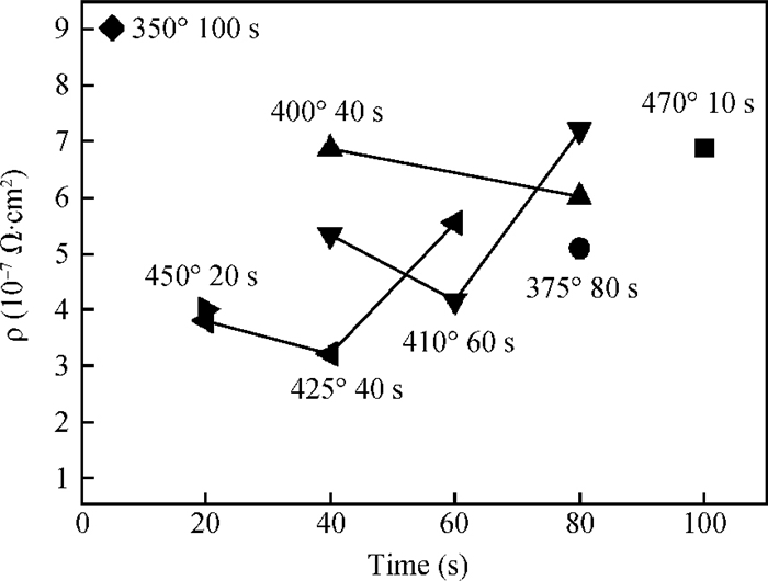
Fig. 1.
Plots of specific contact resistance versus annealing time at various temperatures.
SEMICONDUCTOR TECHNOLOGY
Deqi Wu1, Wuchang Ding1, Shanshan Yang1, 2, Rui Jia1, , Zhi Jin1 and Xinyu Liu1
Corresponding author: Jia Rui, Email:jiarui@ime.ac.cn
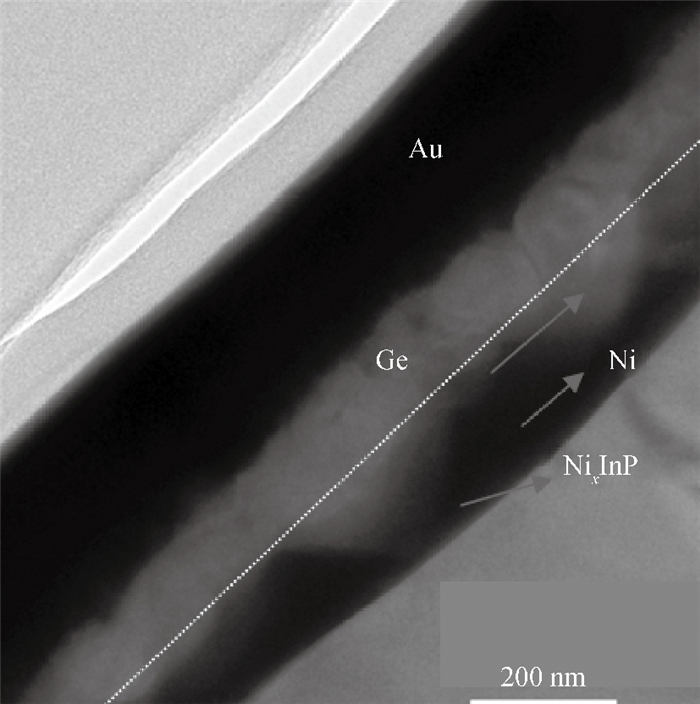
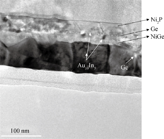
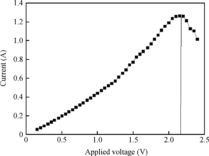
Abstract: The effect of the annealing time and annealing temperature on Ni/Ge/Au electrode contacts deposited on the n-type InP contact layer has been studied using a circular transmission line model. The minimum specific contact resistance of 3.2×10⁻⁷Ω·cm2 was achieved on the low-doped n-type InP contact layer with a 40 s anneal at 425℃. In order to improve the ohmic contact and reduce the difficulty in the fabrication of the high doped InP epi-layer, the doping concentration in the InP contact layer was chosen to be 5×1018 cm-3 in the fabrication of transferred electronic devices. Excellent differential negative resistance properties were obtained by an electron beam evaporating the Ni/Ge/Au/Ge/Ni/Au composite electrode on an InP epi-layer with a 60 s anneal at 380℃.
Keywords: circular transmission line model, specific contact resistance, InP, transferred electronic devices, differential negative resistance
| [1] |
Shih Y C, Murakami M, Wilkie E L, et al. Effects of interfacial microstructure on uniformity and thermal stability of AuNiGe ohmic contact to n-type GaAs. J Appl Phys, 1987, 62:582 doi: 10.1063/1.339860
|
| [2] |
Lin C, Lee C P. Comparison of Au/Ni/Ge, Au/Pd/Ge and Au/Pt/Ge ohmic contacts to n-type GaAs. J Appl Phys, 1990, 67:260 doi: 10.1063/1.345300
|
| [3] |
Ren F, FuUowan T R, Chu S N G, et al. Improved n-type GaAs ohmic contacts compatible with a chlorine-based dry-etch process. J Electron Mater, 1991, 20:305 doi: 10.1007/BF02657895
|
| [4] |
DelAlamo J A, Mizutani T. AuGeNi ohmic contacts to n-InP for FET applications. Solid-State Electron, 1988, 31:1635 doi: 10.1016/0038-1101(88)90011-1
|
| [5] |
Graham R J, Myhajlenko S, Steeds J W. High-resolution luminescence studies of indium phosphide under ohmic contacts. J Appl Phys, 1985, 57:1311 doi: 10.1063/1.334531
|
| [6] |
Anderson D A, Graham R J, Steeds J W. The influence of interfacial morphology and composition on the behaviour of AuGeNi contacts to InP. Semicond Sci Technol, 1988, 3:63 doi: 10.1088/0268-1242/3/2/001
|
| [7] |
Dunn J, Stringfellow G B. Annealed AuGe based ohmic contacts on InP with ion milling prior to metallization. J Electron Mater, 1990, 19:L1 doi: 10.1007/BF02651748
|
| [8] |
Yoder M N. ohmic contacts in GaAs. Solid-state Electron, 1980, 23(2):117 doi: 10.1016/0038-1101(80)90145-8
|
| [9] |
Wu D F, Daembkes H, Heime K. Noneutectic Au/Ge alloy ohmic contact technology for diffused N-channel GaAs MESFET. Journal of Semiconductors, 1984, 5:99 http://www.jos.ac.cn/bdtxbcn/ch/reader/view_abstract.aspx?file_no=200592542371969&flag=1
|
| [10] |
Baca A, Ren F, Zolper J, et al. A survey of ohmic contacts to Ⅲ-Ⅴ compound semiconductors. Thin Solid Films, 1997, 308/309:599 doi: 10.1016/S0040-6090(97)00439-2
|
| [11] |
Dimoulas A, Toriumi A, Mohney S E. Source and drain contacts for germanium and Ⅲ-Ⅴ FETs for digital logic. MRS Bull, 2009, 34:522 doi: 10.1557/mrs2009.140
|
| [12] |
Kim I. Pd/Si-based ohmic contacts to n-type InGaAs for AlGaAs/GaAs HBTs. Mater Lett, 2004, 58:1107 doi: 10.1016/j.matlet.2003.09.001
|
| [13] |
Yearsley J D, Lin J C, Hwang E, et al. Ultra low-resistance palladium silicide ohmic contacts to lightly doped n-InGaAs. J Appl Phys, 2012, 112:054510 doi: 10.1063/1.4748178
|
| [14] |
Marlow G S, Das M B. The effects of contact size and non-zero metal resistance on the determination of specific contact resistance. Solid-State Electron, 1982, 25(2):91 doi: 10.1016/0038-1101(82)90036-3
|
| [15] |
Berger H H. Models for contacts to planar devices. Solid-State Electron, 1972, 15(2):145 doi: 10.1016/0038-1101(72)90048-2
|
| [16] |
Anderson D A, Graham R J, Steeds J W. The influence of interfacial morphology and composition on the behaviour of AuGeNi contacts to InP. Semicond Sci Technol, 1988, 3:63 doi: 10.1088/0268-1242/3/2/001
|
| [17] |
Ivey D G, Wang D, Yang D. Au/Ge/Ni ohmic contacts to n-type InP. J Electron Mater, 1994, 23(5):441 doi: 10.1007/BF02671227
|
| [18] |
Ivey D G, Zhang L, Jian P. Interfacial reactions between palladium thin films and InP. J Mater Sci:Mater Electron, 1991, 2:21 doi: 10.1007/BF00695000
|


Article views: 4040 Times PDF downloads: 149 Times Cited by: 0 Times
Received: 14 August 2013 Revised: 11 October 2013 Online: Published: 01 March 2014
| Citation: |
Deqi Wu, Wuchang Ding, Shanshan Yang, Rui Jia, Zhi Jin, Xinyu Liu. Optimization of ohmic contact for InP-based transferred electronic devices[J]. Journal of Semiconductors, 2014, 35(3): 036001. doi: 10.1088/1674-4926/35/3/036001
****
D Q Wu, W C Ding, S S Yang, R Jia, Z Jin, X Y Liu. Optimization of ohmic contact for InP-based transferred electronic devices[J]. J. Semicond., 2014, 35(3): 036001. doi: 10.1088/1674-4926/35/3/036001.

|
| [1] |
Shih Y C, Murakami M, Wilkie E L, et al. Effects of interfacial microstructure on uniformity and thermal stability of AuNiGe ohmic contact to n-type GaAs. J Appl Phys, 1987, 62:582 doi: 10.1063/1.339860
|
| [2] |
Lin C, Lee C P. Comparison of Au/Ni/Ge, Au/Pd/Ge and Au/Pt/Ge ohmic contacts to n-type GaAs. J Appl Phys, 1990, 67:260 doi: 10.1063/1.345300
|
| [3] |
Ren F, FuUowan T R, Chu S N G, et al. Improved n-type GaAs ohmic contacts compatible with a chlorine-based dry-etch process. J Electron Mater, 1991, 20:305 doi: 10.1007/BF02657895
|
| [4] |
DelAlamo J A, Mizutani T. AuGeNi ohmic contacts to n-InP for FET applications. Solid-State Electron, 1988, 31:1635 doi: 10.1016/0038-1101(88)90011-1
|
| [5] |
Graham R J, Myhajlenko S, Steeds J W. High-resolution luminescence studies of indium phosphide under ohmic contacts. J Appl Phys, 1985, 57:1311 doi: 10.1063/1.334531
|
| [6] |
Anderson D A, Graham R J, Steeds J W. The influence of interfacial morphology and composition on the behaviour of AuGeNi contacts to InP. Semicond Sci Technol, 1988, 3:63 doi: 10.1088/0268-1242/3/2/001
|
| [7] |
Dunn J, Stringfellow G B. Annealed AuGe based ohmic contacts on InP with ion milling prior to metallization. J Electron Mater, 1990, 19:L1 doi: 10.1007/BF02651748
|
| [8] |
Yoder M N. ohmic contacts in GaAs. Solid-state Electron, 1980, 23(2):117 doi: 10.1016/0038-1101(80)90145-8
|
| [9] |
Wu D F, Daembkes H, Heime K. Noneutectic Au/Ge alloy ohmic contact technology for diffused N-channel GaAs MESFET. Journal of Semiconductors, 1984, 5:99 http://www.jos.ac.cn/bdtxbcn/ch/reader/view_abstract.aspx?file_no=200592542371969&flag=1
|
| [10] |
Baca A, Ren F, Zolper J, et al. A survey of ohmic contacts to Ⅲ-Ⅴ compound semiconductors. Thin Solid Films, 1997, 308/309:599 doi: 10.1016/S0040-6090(97)00439-2
|
| [11] |
Dimoulas A, Toriumi A, Mohney S E. Source and drain contacts for germanium and Ⅲ-Ⅴ FETs for digital logic. MRS Bull, 2009, 34:522 doi: 10.1557/mrs2009.140
|
| [12] |
Kim I. Pd/Si-based ohmic contacts to n-type InGaAs for AlGaAs/GaAs HBTs. Mater Lett, 2004, 58:1107 doi: 10.1016/j.matlet.2003.09.001
|
| [13] |
Yearsley J D, Lin J C, Hwang E, et al. Ultra low-resistance palladium silicide ohmic contacts to lightly doped n-InGaAs. J Appl Phys, 2012, 112:054510 doi: 10.1063/1.4748178
|
| [14] |
Marlow G S, Das M B. The effects of contact size and non-zero metal resistance on the determination of specific contact resistance. Solid-State Electron, 1982, 25(2):91 doi: 10.1016/0038-1101(82)90036-3
|
| [15] |
Berger H H. Models for contacts to planar devices. Solid-State Electron, 1972, 15(2):145 doi: 10.1016/0038-1101(72)90048-2
|
| [16] |
Anderson D A, Graham R J, Steeds J W. The influence of interfacial morphology and composition on the behaviour of AuGeNi contacts to InP. Semicond Sci Technol, 1988, 3:63 doi: 10.1088/0268-1242/3/2/001
|
| [17] |
Ivey D G, Wang D, Yang D. Au/Ge/Ni ohmic contacts to n-type InP. J Electron Mater, 1994, 23(5):441 doi: 10.1007/BF02671227
|
| [18] |
Ivey D G, Zhang L, Jian P. Interfacial reactions between palladium thin films and InP. J Mater Sci:Mater Electron, 1991, 2:21 doi: 10.1007/BF00695000
|

 WeChat ID
Journal of Semiconductors © 2017 All Rights Reserved 京ICP备05085259号-2

 DownLoad: