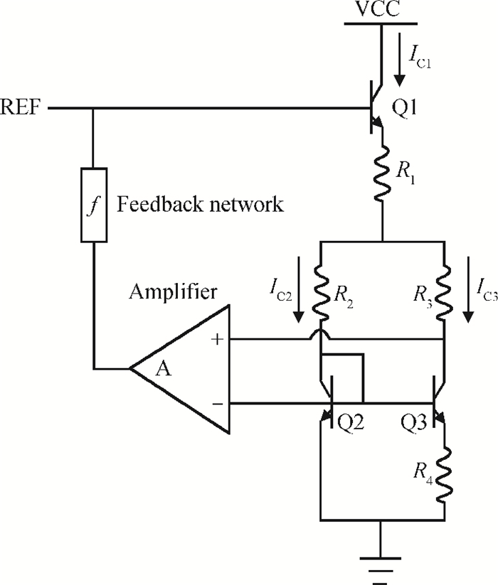
Loading [MathJax]/jax/output/HTML-CSS/jax.js
J. Semicond. > 2014, Volume 35 > Issue 4 > 045008

SEMICONDUCTOR INTEGRATED CIRCUITS

Compact trimming design of a high-precision reference

Guodong Ren, Shifang Zhao, Zhongshen Pu and Zhiqiang Wei

+ Author Affiliations

 Corresponding author: Ren Guodong, Email:rengd@lut.cn

DOI: 10.1088/1674-4926/35/4/045008

PDF

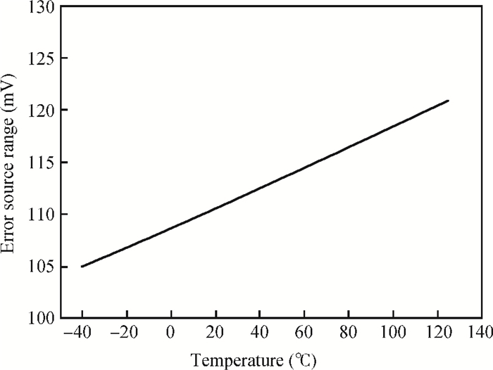
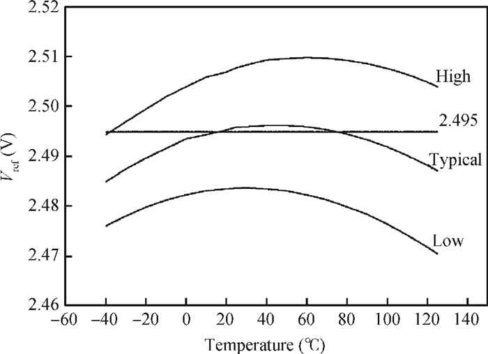
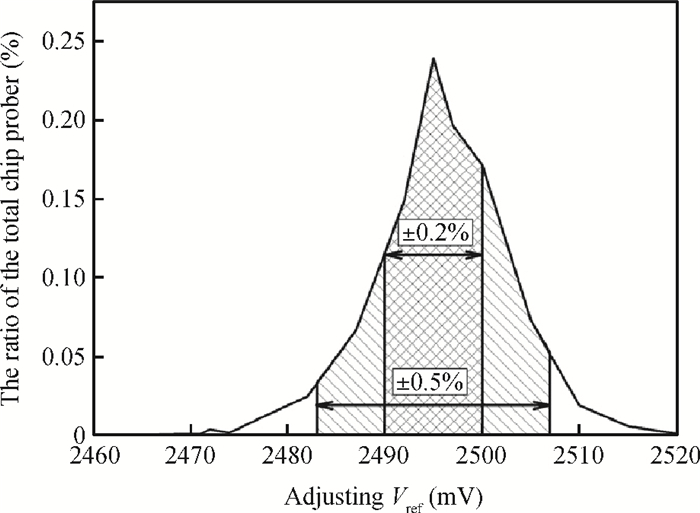
Abstract: To design a high-precision reference, the various error sources have been analyzed and compensated with a compact 111 mV resistor-trim scheme and the upper and lower extremes of the reference precision are also temperature-compensated. At room temperature, the yield of ±0.5% precision is 96% and ±0.2% is 78%.

Key words: high-precisionerror sourcestrimtemperature-compensated

At present, a bandgap reference circuit has been used as a basic block in integrated circuits[1-7]. The reference will directly affect the accuracy of the whole circuit system. Therefore, the study of various error sources that exist in the reference and compensation of this error is particularly important. Here, according to the ideas of Gupta and Rincón-Mora who have studied them, is the given trimming scheme[8].

In the bandgap reference, there are many factors that will give rise to precision errors, such as, base-emitter voltage spread and matching of the transistor, tolerances and resistor[8]. Unfortunately, these errors are inevitable. In order to solve these error sources and obtain high-precision components, Section 2 will present the analysis and quantitative calculation of each error source. In Section 3, the compact binary-weighted resistor trim schemes were used to compensate the error. The chip prober data is obtained before trimming and after. The conclusion is given in Section 4.

Figure 1 shows the schematic of a bandgap reference circuit in bipolar technology. The voltage drop across R2 and R3 is identical because of the amplifier. The resistance of R3 is 3 times that of R2 and the current flowing in R2 is 3 times that of R3. The current flowing in R1 is the sum of currents. The reference voltage in Fig. 1 is

VREF=VBE1+VBE2+IC2R2+IC1R1,

(1)
Figure  1.  Bandgap reference circuit.

where VBE1 and VBE2 are the base-emitter voltage of transistors Q1 and Q2. IC1 and IC2 are the current flowing through resistors R1 and R2. Equation (1) can be written as

VREF=VTlnIC1IS1+VTlnIC2IS2+(VTR4R3R2lnC)R2+(VTR4R3R2lnC+VTR4lnC)R1,

(2)

where C is the ratio of the current densities of Q2 and Q3.

By applying the mathematical analysis of error sources to Eq. (2), the derivative of the reference voltage is given as

ΔVREF=VBE1IS1ΔIS1+VBE2IS2ΔIS2+VBE1IC1ΔIC1+VBE2IC2ΔIC2+IC2R2R4ΔR4+IC2R2CΔC+IC2R2R3/R2ΔR3R2+IC2R2R2/R4ΔR2R4+IC2R2R2ΔR2+IC1R1R4ΔR4+IC1R1CΔC+IC1R1R1/R4ΔR1R4+IC1R1R1ΔR1+IC1R1R3/R2ΔR3R2.

(3)

The magnitude of the error in reference VREF is obtained by comparing the reference voltage of an "ideal" reference, where the particular error sources are process-induced. The magnitude of error ΔIS is the error of the transfer characteristic of the transistor, ΔIS = ISδS (δS is the error ratio of the transistor's transfer characteristic). Furthermore, ΔIC1 and ΔIC2 are the collector current errors of the two bipolar transistors Q1 and Q2, and the derivatives of the collector currents are given as

ΔIC1=IC1R4ΔR4+IC1CΔC+IC1R3/R2ΔR3R2IC1R4ΔR4+(1+R3R2)VTR41CΔC,

(4)

ΔIC2=IC2R4ΔR4+IC2CΔC+IC2R3/R2ΔR3R2IC2R4ΔR4+R3R2VTR41CΔC,

(5)

where the factors that the errors of resistor R4, C and matching resistor R3/R2 give rise to ΔIC1 and ΔIC2, then Equations (4) and (5) have described them. The magnitude error of R4 is ΔR4 = R4δRA (δRA is the error ratio of resistor tolerance). The magnitude error of C is ΔC=CδNPN (δNPN is the error ratio of the transistor matching[8]. The matching tolerance of resistors R3/R2 is negligible due to their ratio. In layout, identical resistor geometries are used[9]. Namely, the resistor R3 is 3 times that of the resistor R2, and this allows ways to be devised to minimize the matching error of the pair of resistors.

The tolerances of resistors R1 and R2 are ΔR1 = R1δRA, ΔR2 = R2δRA. The matching tolerance exists in the pair of resistors. While the matching error of pairs R1/R4 and R2/R4 is larger than the R3/R2 pair of resistors, they are significant. They can be described as ΔR1/R4 = R1/R4 × δRR, ΔR2/R4 = R2/R4 × δRR (δRR is the error ratio of resistor matching tolerance). By substituting Eqs. (4), (5) and other parameter tolerances into Eq. (3), the error of the reference voltage is given by

ΔVREF=2ΔVBE2VTδRA+2VTlnCδNPN+3VTR4R2δNPN+4VTR4R1δNPN+3VTlnCR2R4δRR+4VTlnCR1R4δRR,

(6)

where -2ΔVBE is the transistors of the Q1 and Q2 base-emitter voltage spread, 3VTlnC × (R2/R4) × δRR + 4VTlnC × (R1/R4) × δRR is the resistor matching tolerances, -2VT δRA is the resistor tolerances and 2VT/lnC × δNPN + 3VT(R2/R4) × δNPN + 4VT(R1/R4) × δNPN is the matching tolerances of the transistors.

VBE spread is the considerable error source and is critical because it exists in process biases. A number of factors give rise to this error, such as the width of the base WB, the cross-sectional area of the emitter A, the equilibrium concentration of electrons in the base np0, the diffusion capacity for electrons Dn, and etc[10]. These parameters are constants according to the ideal state in a general quantitative calculation. In fact, these parameters will deviate from the ideal values. They will be directly reflected in the error of the reference voltage, the value is ΔVBE=±24 mV[11]. By substituting the ΔVBE values into part of Eq. (6) using VBE spread, the following results can be obtained

ΔVREF=±48mV.

(7)

The references use matched bipolar transistors Q2 and Q3 to produce known voltages and currents. This error source comes from matched bipolar transistors Q2 and Q3. NPN collector currents scale approximately with the drawn emitter area, the mismatch of them between a pair of transistors is due to the emitter area fluctuations[8]. By substituting the δNPN value into part of Eq. (6) using the matching tolerances of the transistors, at room temperature, the error in the reference voltage is given by

ΔVREF=2VTlnCδNPN+3VTR2R4δNPN+4VTR1R4δNPN.

(8)

During the production of devices, resistor tolerances will trigger a change of the current thereby directly causing a transistor base-emitter voltage change ΔVBE and the collector current changes ΔIC. The value of δRA is 20%[8]. By substituting the δRA values into part of Eq. (6) using resistor tolerances, at room temperature, the following results can be obtained:

ΔVREF=2VTδRA.

(9)

Resistors with different widths, lengths or shapes can easily experience mismatches of ±1% or more, and they are not neglected. When designing the layout, some matching rules can be applied for each process to obtain matched devices with a desired degree of accuracy. In the quantitative calculation, these resistor matching tolerances will not disappear.

δRR is the ratio of resistor matching tolerance. We assume that these contacts have a process bias of 0.2 μm[8]. Considering the case of matched resistors having the same widths of 6 μm, if the matched resistors R1, R2, R4 were 114 μm, 68.4 μm, 27 μm long, respectively, then the mismatch caused by this bias would equal 4.191, 2.522, δRR represents an about 2% mismatch of the resistors. Substitution of the δRR values into part of Eq. (6) by resistor matching tolerances, at room temperature, the following results can be obtained:

ΔVREF=3VTlnCR2δRRR4+4VTlnCR1δRRR4.

(10)

The previous sections have described the various error sources responsible for causing the base-emitter voltage spread and matching of the transistor, tolerances and matching of the resistor and transistor. If each parameter value is substituted into Eqs. (7)-(10), the analytic value of every error source will be calculated. At room temperature, the transistors of the Q1 and Q2 base-emitter voltage spread is constant (±24 mV), the resistor matching tolerance is 13.34 mV, the resistor tolerance is -10 mV and the transistor matching tolerance is 22.85 mV. The total trimming voltage is 111 mV according to the calculated RMSE ±55.71 mV. From Eq. (6), the error of the reference is the linear function to the temperature. It can be described as Fig. 2.

Figure  2.  Total trimming voltage versus temperature.

Figure 3 shows the simulation results from the analytical value of reference. At room temperature (Tr), the typical reference is 2.495 V[12], the fast and slow voltages are 2.508 V and 2.483 V with the 111 mV trimming. The upper and lower extremes of the reference precision are compensated to temperature because the reference is compensated. To the lower extreme of precision, the worst case exists at the limiting temperature and the upper at 60 ℃.

Figure  3.  Reference voltage versus temperature.

In Fig. 4, the binary-weighted series-connected resistor trim schemes can minimize the error sources. The binary-weighted resistor is 312 Ω/156 Ω/78 Ω/39 Ω with respect to extra voltage 56 mV/28 mV/14 mV/7 mV. However, the actual voltage is 60 mV/30 mV/14 mV/7 mV because of the additional contact resistor. The sum of extra voltage is the trim range.

Figure  4.  The binary-weighted series-connected resistor trim schemes using fuses.

Before trimming, the typical reference is 2.405 V and the interval is [2.330, 2.510]. All chip prober values can form the normal distribution as shown in Fig. 5. The horizontal axis shows the testing reference voltage, and the vertical axis shows the ratio of the total of the chip prober. On the curve, the values around 2.405 V are valid, and others are invalid from the edge of the wafer.

Figure  5.  CP value before adjusting.

All of the defective dice will be trimmed during the chip probe. In Fig. 6, the data is shown after trimming. According to the design requirement of ±0.5% precision, the interval of the reference voltage is [2.483, 2.507] by the given typical value 2.495 V. The total chip-prober samples are 33560, whereas 32261 samples satisfy the request. The yield exceeds 96% and 78% of the total samples exist in the interval [2.490, 2.500] where the precision is about ±0.2%. In Table 1, the reference is measured from room temperature to 125 ℃.

Figure  6.  CP value after adjusting.
Table  1.  The measured reference voltage.
DownLoad: CSV  | Show Table

The 4-bit binary-weighted series-connected resistor trim scheme is used to compensate the error sources in which the base-emitter voltage spread is the main error source and the others are affected by temperature. The precision of the reference is temperature-compensated because the reference is temperature-compensated.


[1]
Basso C, Kadanka P. The TL431 in switch-mode power supplies loops:part Ⅰ. Electronic Design and Application World-Nikkei Electronics China, 2009, (3):99
[2]
Meijer G C, Wang G, Fruett F. Temperature sensors and voltage references implemented in COMS technology. IEEE J Sensors, 2001, 1(3):225 doi: 10.1109/JSEN.2001.954835
[3]
Palumbo G. Voltage references from diodes to precision high-order bandgap circuits. IEEE Circuits and Devices Magazine, 2002, 18(5):45 doi: 10.1109/MCD.2002.1035357
[4]
Song B S, Gray P R. A precision curvature-compensated CMOS bandgap reference. IEEE J Solid-State Circuits, 1983, 18(6):634 doi: 10.1109/JSSC.1983.1052013
[5]
Meijer G M, Fonderie C. A curvature-corrected low-voltage bandgap reference. IEEE J Solid-State Circuits, 1993, 28(6):667 doi: 10.1109/4.217981
[6]
Sheng Jinggang, Chen Zhiliang, Shi Bingxue. A CMOS bandgap reference with 1 V supply. Chinese Journal of Semiconductors, 2005, 26(4):826 https://www.researchgate.net/publication/293255783_CMOS_bandgap_reference_with_1V_supply
[7]
Xu Yong, Wang Zhigong, Guan Yu. Improved design of a bandgap voltage reference with high accuracy. Chinese Journal of Semiconductors, 2006, 27(12):2209 https://www.researchgate.net/publication/291296647_Improved_design_of_a_bandgap_voltage_reference_with_high_accuracy
[8]
Gupta V, Rincón-Mora G A. Predicting and designing for the impact of process variations and mismatch on the trim range and yield of bandgap reference. Quality of Electronic Design, 2005:503 http://dl.acm.org/citation.cfm?id=1049711&CFID=426924195&CFTOKEN=68355621
[9]
Hastings A. The art of analog layout. Beijing:Tsinghua University Press, 2004
[10]
Anderson B L, Anderson R L. Fundamentals of semiconductor devices. Beijing:Tsinghua University Press, 2006
[11]
Gupta V, Rincón-Mora G A. Predicting the effects of error sources in bandgap reference circuits and evaluating their design implications. Circuits and Systems, 2002, 3:575 http://ieeexplore.ieee.org/xpls/icp.jsp?arnumber=1187105
[12]
TLV431 Datasheet[c]. 2000-2005 Texas Instruments Incorporated
Fig. 1.  Bandgap reference circuit.

Fig. 2.  Total trimming voltage versus temperature.

Fig. 3.  Reference voltage versus temperature.

Fig. 4.  The binary-weighted series-connected resistor trim schemes using fuses.

Fig. 5.  CP value before adjusting.

Fig. 6.  CP value after adjusting.

Table 1.   The measured reference voltage.

[1]
Basso C, Kadanka P. The TL431 in switch-mode power supplies loops:part Ⅰ. Electronic Design and Application World-Nikkei Electronics China, 2009, (3):99
[2]
Meijer G C, Wang G, Fruett F. Temperature sensors and voltage references implemented in COMS technology. IEEE J Sensors, 2001, 1(3):225 doi: 10.1109/JSEN.2001.954835
[3]
Palumbo G. Voltage references from diodes to precision high-order bandgap circuits. IEEE Circuits and Devices Magazine, 2002, 18(5):45 doi: 10.1109/MCD.2002.1035357
[4]
Song B S, Gray P R. A precision curvature-compensated CMOS bandgap reference. IEEE J Solid-State Circuits, 1983, 18(6):634 doi: 10.1109/JSSC.1983.1052013
[5]
Meijer G M, Fonderie C. A curvature-corrected low-voltage bandgap reference. IEEE J Solid-State Circuits, 1993, 28(6):667 doi: 10.1109/4.217981
[6]
Sheng Jinggang, Chen Zhiliang, Shi Bingxue. A CMOS bandgap reference with 1 V supply. Chinese Journal of Semiconductors, 2005, 26(4):826 https://www.researchgate.net/publication/293255783_CMOS_bandgap_reference_with_1V_supply
[7]
Xu Yong, Wang Zhigong, Guan Yu. Improved design of a bandgap voltage reference with high accuracy. Chinese Journal of Semiconductors, 2006, 27(12):2209 https://www.researchgate.net/publication/291296647_Improved_design_of_a_bandgap_voltage_reference_with_high_accuracy
[8]
Gupta V, Rincón-Mora G A. Predicting and designing for the impact of process variations and mismatch on the trim range and yield of bandgap reference. Quality of Electronic Design, 2005:503 http://dl.acm.org/citation.cfm?id=1049711&CFID=426924195&CFTOKEN=68355621
[9]
Hastings A. The art of analog layout. Beijing:Tsinghua University Press, 2004
[10]
Anderson B L, Anderson R L. Fundamentals of semiconductor devices. Beijing:Tsinghua University Press, 2006
[11]
Gupta V, Rincón-Mora G A. Predicting the effects of error sources in bandgap reference circuits and evaluating their design implications. Circuits and Systems, 2002, 3:575 http://ieeexplore.ieee.org/xpls/icp.jsp?arnumber=1187105
[12]
TLV431 Datasheet[c]. 2000-2005 Texas Instruments Incorporated
1

Observation of exciton polariton condensation in a perovskite lattice at room temperature

Jun Zhang

Journal of Semiconductors, 2020, 41(3): 030201. doi: 10.1088/1674-4926/41/3/030201

2

High Curie temperature ferromagnetism and high hole mobility in tensile strained Mn-doped SiGe thin films

Jianhua Zhao

Journal of Semiconductors, 2020, 41(8): 080201. doi: 10.1088/1674-4926/41/8/080201

3

Fabrication of room temperature continuous-wave operation GaN-based ultraviolet laser diodes

Degang Zhao, Jing Yang, Zongshun Liu, Ping Chen, Jianjun Zhu, et al.

Journal of Semiconductors, 2017, 38(5): 051001. doi: 10.1088/1674-4926/38/5/051001

4

Substrate temperature dependent studies on properties of chemical spray pyrolysis deposited CdS thin films for solar cell applications

Kiran Diwate, Amit Pawbake, Sachin Rondiya, Rupali Kulkarni, Ravi Waykar, et al.

Journal of Semiconductors, 2017, 38(2): 023001. doi: 10.1088/1674-4926/38/2/023001

5

Variable range hopping conduction in n-CdSe samples at very low temperature

M Errai, A El Kaaouachi, H El Idrissi

Journal of Semiconductors, 2015, 36(12): 122001. doi: 10.1088/1674-4926/36/12/122001

6

Effect of substrate temperature on the stability of transparent conducting cobalt doped ZnO thin films

Said Benramache, Boubaker Benhaoua, Foued Chabane

Journal of Semiconductors, 2012, 33(9): 093001. doi: 10.1088/1674-4926/33/9/093001

7

A process/temperature variation tolerant RSSI

Lei Qianqian, Lin Min, Shi Yin

Journal of Semiconductors, 2012, 33(12): 125010. doi: 10.1088/1674-4926/33/12/125010

8

Structural and optoelectronic properties of sprayed Sb:SnO2 thin films: Effects of substrate temperature and nozzle-to-substrate distance

A. R. Babar, S. S. Shinde, A. V. Moholkar, C. H. Bhosale, K. Y. Rajpure, et al.

Journal of Semiconductors, 2011, 32(10): 102001. doi: 10.1088/1674-4926/32/10/102001

9

A high precision high PSRR bandgap reference with thermal hysteresis protection

Yang Yintang, Li Yani, Zhu Zhangming

Journal of Semiconductors, 2010, 31(9): 095010. doi: 10.1088/1674-4926/31/9/095010

10

High temperature characterization of double base epilayer 4H-SiC BJTs

Zhang Qian, Zhang Yuming, Zhang Yimen, Wang Yuehu

Journal of Semiconductors, 2010, 31(11): 114005. doi: 10.1088/1674-4926/31/11/114005

11

A novel precision curvature-compensated bandgap reference

Zhou Zekun, Ming Xin, Zhang Bo, Li Zhaoji

Journal of Semiconductors, 2010, 31(1): 015010. doi: 10.1088/1674-4926/31/1/015010

12

Temperature self-adaptive program algorithm on 65 nm MLC NOR flash memory

Shi Weihua, Hong Zhiliang, Hu Chaohong, Kang Yong

Journal of Semiconductors, 2009, 30(8): 085012. doi: 10.1088/1674-4926/30/8/085012

13

Temperature: a critical parameter affecting the optical properties of porous silicon

Long Yongfu, Ge Jin, Ding Xunmin, Hou Xiaoyuan

Journal of Semiconductors, 2009, 30(6): 063002. doi: 10.1088/1674-4926/30/6/063002

14

An ultra-low-power CMOS temperature sensor for RFID applications

Xu Conghui, Gao Peijun, Che Wenyi, Tan Xi, Yan Na , et al.

Journal of Semiconductors, 2009, 30(4): 045003. doi: 10.1088/1674-4926/30/4/045003

15

A high precision programmable bandgap voltage reference design for high resolution ADC

Zhu Tiancheng, Yao Suying, Li Binqiao

Journal of Semiconductors, 2009, 30(7): 075005. doi: 10.1088/1674-4926/30/7/075005

16

High-temperature characteristics of AlxGa1–xN/GaN Schottky diodes

Zhang Xiaoling, Li Fei, Lu Changzhi, Xie Xuesong, Li Ying, et al.

Journal of Semiconductors, 2009, 30(3): 034001. doi: 10.1088/1674-4926/30/3/034001

17

High quality AlGaN grown on a high temperature AlN template by MOCVD

Yan Jianchang, Wang Junxi, Liu Naixin, Liu Zhe, Ruan Jun, et al.

Journal of Semiconductors, 2009, 30(10): 103001. doi: 10.1088/1674-4926/30/10/103001

18

Temperature Distribution in Ridge Structure InGaN Laser Diodes and Its Influence on Device Characteristics

Li Deyao, Huang Yongzhen, Zhang Shuming, Chong Ming, Ye Xiaojun, et al.

Chinese Journal of Semiconductors , 2006, 27(3): 499-505.

19

Temperature Dependence of Vacuum Rabi Splitting in a Single Quantum Dot-Semiconductor Microcavity

Zhu Kadi, Li Waisang

Chinese Journal of Semiconductors , 2006, 27(3): 489-493.

20

Room Temperature Operation of Strain-Compensated 5.5μm Quantum Cascade Lasers

Lu Xiuzhen, Liu Fengqi, Liu Junqi, Jin Peng, Wang Zhanguo, et al.

Chinese Journal of Semiconductors , 2005, 26(12): 2267-2270.

  • Search

    Advanced Search >>

    GET CITATION

    Guodong Ren, Shifang Zhao, Zhongshen Pu, Zhiqiang Wei. Compact trimming design of a high-precision reference[J]. Journal of Semiconductors, 2014, 35(4): 045008. doi: 10.1088/1674-4926/35/4/045008
    G D Ren, S F Zhao, Z S Pu, Z Q Wei. Compact trimming design of a high-precision reference[J]. J. Semicond., 2014, 35(4): 045008. doi: 10.1088/1674-4926/35/4/045008.
    shu

    Export: BibTex EndNote

    Article Metrics

    Article views: 2443 Times PDF downloads: 13 Times Cited by: 0 Times

    History

    Received: 25 September 2013 Revised: 16 November 2013 Online: Published: 01 April 2014

    Catalog

      Email This Article

      User name:
      Email:*请输入正确邮箱
      Code:*验证码错误
      Guodong Ren, Shifang Zhao, Zhongshen Pu, Zhiqiang Wei. Compact trimming design of a high-precision reference[J]. Journal of Semiconductors, 2014, 35(4): 045008. doi: 10.1088/1674-4926/35/4/045008 ****G D Ren, S F Zhao, Z S Pu, Z Q Wei. Compact trimming design of a high-precision reference[J]. J. Semicond., 2014, 35(4): 045008. doi: 10.1088/1674-4926/35/4/045008.
      Citation:
      Guodong Ren, Shifang Zhao, Zhongshen Pu, Zhiqiang Wei. Compact trimming design of a high-precision reference[J]. Journal of Semiconductors, 2014, 35(4): 045008. doi: 10.1088/1674-4926/35/4/045008 ****
      G D Ren, S F Zhao, Z S Pu, Z Q Wei. Compact trimming design of a high-precision reference[J]. J. Semicond., 2014, 35(4): 045008. doi: 10.1088/1674-4926/35/4/045008.

      Compact trimming design of a high-precision reference

      DOI: 10.1088/1674-4926/35/4/045008
      Funds:

      the National Natural Science Foundation of China 61366006

      Project supported by the National Natural Science Foundation of China (Nos. 61366006, No.51261015) and the Natural Science Foundation of Gansu (No. 1308RJZA238)

      the National Natural Science Foundation of China 51261015

      the Natural Science Foundation of Gansu 1308RJZA238

      More Information
      • Corresponding author: Ren Guodong, Email:rengd@lut.cn
      • Received Date: 2013-09-25
      • Revised Date: 2013-11-16
      • Published Date: 2014-04-01

      Catalog

        /

        DownLoad:  Full-Size Img  PowerPoint
        Return
        Return