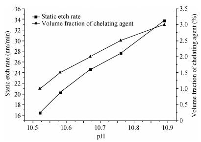
Fig. 1.
The curve of the static etch rate with different pH adjusted by FA/O II chelate agent.
SEMICONDUCTOR MATERIALS
Haokun Yang, Yuling Liu, Ming Sun and Yingde Li
Corresponding author: Yang Haokun,Email:yang.haokun@hotmail.com
Abstract: The oxidation induced stacking faults (OISFs) exposed on the surface of polished silicon substrate are harmful to the electrical performance and reliability of the device region located on the wafer surface. This work investigates the characteristics of the novel nano colloidal silica alkaline slurry, including polyamine and complex non-ions surface surfactant. The experimental results show that when the pH value is higher than 10.1, the removal rate can be higher than 750 nm/min and the surface roughness can be lower than 0.3 nm (10×10 μm2). The surface OISFs existing on the wafer are efficiently controlled with the slurry, and the defect density on the polished wafer surface decreases greatly as well.
Keywords: silicon, oxidation induced stacking fault, chemical mechanical polishing, defect density
| [1] |
Kamia S, Iise H, Nagaike T, et al. Microstructural analysis for Si wafer after CMG process. Key Eng Mater, 2007:329
|
| [2] |
Eda H, Zhou L, Nakano H, et al. Development of single step grinding system for large scale φ 300 Si wafer:a total integrated fixed-abrasive solution. CIRP Ann Manuf Tech, 2001, 50:225 doi: 10.1016/S0007-8506(07)62110-6
|
| [3] |
Pei Z J, Fisher G R, Bhagavat M, et al. A grinding-based manufacturing method for silicon wafers:an experimental investigation. Int J Machine Tools Manuf, 2005, 45:1140 doi: 10.1016/j.ijmachtools.2004.12.006
|
| [4] |
Han Haijian, Zhou Qigang, Dai Xiaolin. Effects of nitrogen on oxidation induced stacking faults in 300 mm CZ silicon. Chinese Journal of Rare Metals, 2009, 33(2):223
|
| [5] |
Smyntyna V A, Sviridova O V. Genesis of initial defects in the process of monocrystalline silicon oxidation with subsequent scribing. Lashkaryov Institute of Semiconductor Physics, National Academy of Sciences of Ukraine, 2010, 13(1):74
|
| [6] |
Que Duanlin. Nitrogen in CZ silicon. Journal of Synthetic Crystals, 2000, 29(5):3
|
| [7] |
Chen Jiahe. Microdefects and defect engineering of iso-group elements doped Czochralski silicon used for large-scale integrated circuits. Hangzhou:Zhejiang University, 2008
|
| [8] |
Falster R, Gambaro D, Olmo M, et al. Non-destructive diagnostic techniques for oxygen precipitates in Czochralski silicon. Mater Res Soc Symp Proc, 1998, 510:27 doi: 10.1557/PROC-510-27
|
| [9] |
Falster R, Fisher G R, Ferrero G. On the properties of rhe intrinsic point defecis in silicon:a perspective from crystal growth and wafer processing. Appl Phys Lett, 1991, 59:809 doi: 10.1063/1.105350
|
| [10] |
GB/T 1031-2009 Geometrical product specifications (GPS)-Surface texture:Profile method-Surface roughness parameters and their values
|
| [11] |
GB/T 3505-2009 Geometrical product specifications (GPS)-Surface texture:Profile method-Terms, definitions and surface texture parameters
|
| [12] |
GB/T 4058-2009 Test method for detection of oxidation induced defects in polished silicon wafers
|
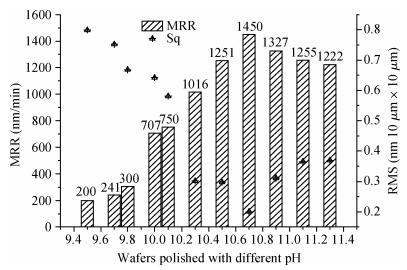
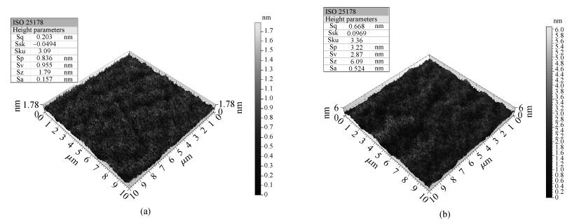
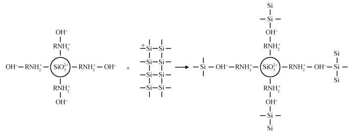
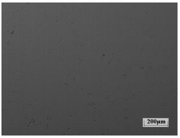
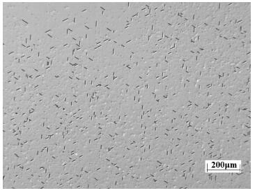
Table 1. Polishing process parameters.

|
| [1] |
Kamia S, Iise H, Nagaike T, et al. Microstructural analysis for Si wafer after CMG process. Key Eng Mater, 2007:329
|
| [2] |
Eda H, Zhou L, Nakano H, et al. Development of single step grinding system for large scale φ 300 Si wafer:a total integrated fixed-abrasive solution. CIRP Ann Manuf Tech, 2001, 50:225 doi: 10.1016/S0007-8506(07)62110-6
|
| [3] |
Pei Z J, Fisher G R, Bhagavat M, et al. A grinding-based manufacturing method for silicon wafers:an experimental investigation. Int J Machine Tools Manuf, 2005, 45:1140 doi: 10.1016/j.ijmachtools.2004.12.006
|
| [4] |
Han Haijian, Zhou Qigang, Dai Xiaolin. Effects of nitrogen on oxidation induced stacking faults in 300 mm CZ silicon. Chinese Journal of Rare Metals, 2009, 33(2):223
|
| [5] |
Smyntyna V A, Sviridova O V. Genesis of initial defects in the process of monocrystalline silicon oxidation with subsequent scribing. Lashkaryov Institute of Semiconductor Physics, National Academy of Sciences of Ukraine, 2010, 13(1):74
|
| [6] |
Que Duanlin. Nitrogen in CZ silicon. Journal of Synthetic Crystals, 2000, 29(5):3
|
| [7] |
Chen Jiahe. Microdefects and defect engineering of iso-group elements doped Czochralski silicon used for large-scale integrated circuits. Hangzhou:Zhejiang University, 2008
|
| [8] |
Falster R, Gambaro D, Olmo M, et al. Non-destructive diagnostic techniques for oxygen precipitates in Czochralski silicon. Mater Res Soc Symp Proc, 1998, 510:27 doi: 10.1557/PROC-510-27
|
| [9] |
Falster R, Fisher G R, Ferrero G. On the properties of rhe intrinsic point defecis in silicon:a perspective from crystal growth and wafer processing. Appl Phys Lett, 1991, 59:809 doi: 10.1063/1.105350
|
| [10] |
GB/T 1031-2009 Geometrical product specifications (GPS)-Surface texture:Profile method-Surface roughness parameters and their values
|
| [11] |
GB/T 3505-2009 Geometrical product specifications (GPS)-Surface texture:Profile method-Terms, definitions and surface texture parameters
|
| [12] |
GB/T 4058-2009 Test method for detection of oxidation induced defects in polished silicon wafers
|


Article views: 3695 Times PDF downloads: 22 Times Cited by: 0 Times
Received: 20 July 2013 Revised: 24 December 2013 Online: Published: 01 May 2014
| Citation: |
Haokun Yang, Yuling Liu, Ming Sun, Yingde Li. The micro morphology correction function of a silicon wafer CMP surface[J]. Journal of Semiconductors, 2014, 35(5): 053002. doi: 10.1088/1674-4926/35/5/053002
****
H K Yang, Y L Liu, M Sun, Y D Li. The micro morphology correction function of a silicon wafer CMP surface[J]. J. Semicond., 2014, 35(5): 053002. doi: 10.1088/1674-4926/35/5/053002.

|
| [1] |
Kamia S, Iise H, Nagaike T, et al. Microstructural analysis for Si wafer after CMG process. Key Eng Mater, 2007:329
|
| [2] |
Eda H, Zhou L, Nakano H, et al. Development of single step grinding system for large scale φ 300 Si wafer:a total integrated fixed-abrasive solution. CIRP Ann Manuf Tech, 2001, 50:225 doi: 10.1016/S0007-8506(07)62110-6
|
| [3] |
Pei Z J, Fisher G R, Bhagavat M, et al. A grinding-based manufacturing method for silicon wafers:an experimental investigation. Int J Machine Tools Manuf, 2005, 45:1140 doi: 10.1016/j.ijmachtools.2004.12.006
|
| [4] |
Han Haijian, Zhou Qigang, Dai Xiaolin. Effects of nitrogen on oxidation induced stacking faults in 300 mm CZ silicon. Chinese Journal of Rare Metals, 2009, 33(2):223
|
| [5] |
Smyntyna V A, Sviridova O V. Genesis of initial defects in the process of monocrystalline silicon oxidation with subsequent scribing. Lashkaryov Institute of Semiconductor Physics, National Academy of Sciences of Ukraine, 2010, 13(1):74
|
| [6] |
Que Duanlin. Nitrogen in CZ silicon. Journal of Synthetic Crystals, 2000, 29(5):3
|
| [7] |
Chen Jiahe. Microdefects and defect engineering of iso-group elements doped Czochralski silicon used for large-scale integrated circuits. Hangzhou:Zhejiang University, 2008
|
| [8] |
Falster R, Gambaro D, Olmo M, et al. Non-destructive diagnostic techniques for oxygen precipitates in Czochralski silicon. Mater Res Soc Symp Proc, 1998, 510:27 doi: 10.1557/PROC-510-27
|
| [9] |
Falster R, Fisher G R, Ferrero G. On the properties of rhe intrinsic point defecis in silicon:a perspective from crystal growth and wafer processing. Appl Phys Lett, 1991, 59:809 doi: 10.1063/1.105350
|
| [10] |
GB/T 1031-2009 Geometrical product specifications (GPS)-Surface texture:Profile method-Surface roughness parameters and their values
|
| [11] |
GB/T 3505-2009 Geometrical product specifications (GPS)-Surface texture:Profile method-Terms, definitions and surface texture parameters
|
| [12] |
GB/T 4058-2009 Test method for detection of oxidation induced defects in polished silicon wafers
|

 WeChat ID
Journal of Semiconductors © 2017 All Rights Reserved 京ICP备05085259号-2

 DownLoad: