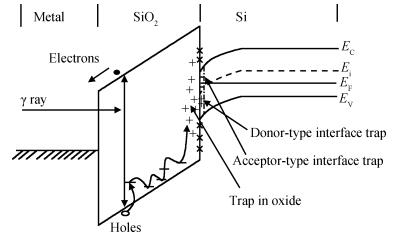
Fig. 1.
An energy band diagram for MOS structure during irradiation with positive bias on the gate and electron-hole motion.
SEMICONDUCTOR DEVICES
Zhaohuan Tang1, , Rongkan Liu2, Kaizhou Tan1, Jun Luo2, Gangyi Hu1, Ruzhang Li1, Huaping Ren3 and Bin Wang2
Corresponding author: Tang Zhaohuan, Email:sisc_tang@163.com
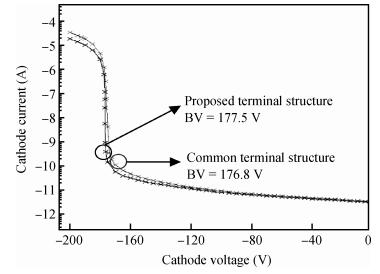
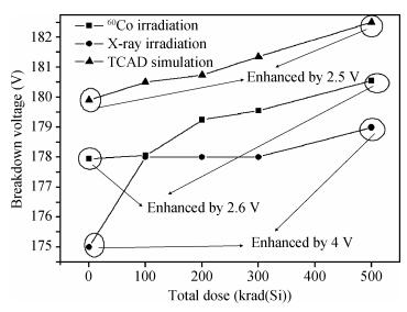
Abstract: Using positive surface charge instead of traditional γ-ray total dose irradiation, the electric field distribution of a P-channel VDMOS terminal has been analyzed. A novel terminal structure for improving the total dose irradiation hardened of P-channel VDMOS has been proposed, and the structure is simulated and demonstrated with a -150 V P-channel VDMOS. The results show that the peak current density is reduced from 5.51×10³ A/cm2 to 2.01×10³ A/cm2, and the changed value of the breakdown voltage is 2.5 V at 500 krad(Si). Especially, using 60Co and X-ray to validate the results, which strictly match with the simulated values, there is not any added mask or process to fabricate the novel structure, of which the process is compatible with common P-channel VDMOS processes. The novel terminal structure can be widely used in total irradiation hardened P-channel VDMOS design and fabrication, which holds a great potential application in the space irradiation environment.
Keywords: P-channel VDMOS, total dose irradiation hardened, stop field limited ring, breakdown voltage
| [1] |
Li Zehong, Zhang Lei, Tan Kaizhou. Total dose radiation hardened power VDMOS device. Journal of UESTC, 2008, 37(4):621(in Chinese)
|
| [2] |
Raparla V A K, Lee S C, Schrimpf R D, et al. A model of radiation effects in nitride-oxide films for power MOSFET applications. Solid-State Electron, 2003, 47:775 doi: 10.1016/S0038-1101(02)00375-1
|
| [3] |
Gao Bo, Yu Xuefeng, Ren Diyuan, et al. Total ionizing dose effects and annealing behavior for domestic VDMOS devices. Journal of Semiconductors, 2010, 31(4):044007 doi: 10.1088/1674-4926/31/4/044007
|
| [4] |
Cai Xiaowu, Hai Chaohe, Wang Lixin, et al. Gamma irradiation induced oxide trapped charge and interface charge in power VDMOS. Journal of Functional Material and Devices, 2008, 14(5):621(in Chinese)
|
| [5] |
Xue Yuxiong, Cao Zhou, Guo Zuyou, et al. Study of total ionization dose test of power MOSFET for satellite application. Nuclear Electronics & Detection Technology, 2008, 28(3):538(in Chinese)
|
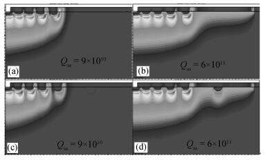
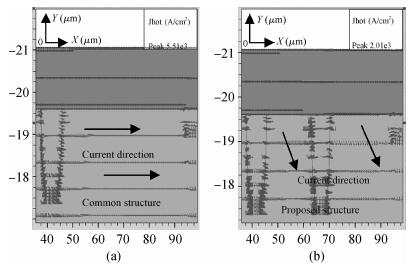
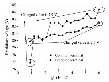
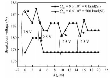
Table 1. Test results of P-VDMOS designed in proposed terminal structure at 0 and 500 krad(Si).

|
| [1] |
Li Zehong, Zhang Lei, Tan Kaizhou. Total dose radiation hardened power VDMOS device. Journal of UESTC, 2008, 37(4):621(in Chinese)
|
| [2] |
Raparla V A K, Lee S C, Schrimpf R D, et al. A model of radiation effects in nitride-oxide films for power MOSFET applications. Solid-State Electron, 2003, 47:775 doi: 10.1016/S0038-1101(02)00375-1
|
| [3] |
Gao Bo, Yu Xuefeng, Ren Diyuan, et al. Total ionizing dose effects and annealing behavior for domestic VDMOS devices. Journal of Semiconductors, 2010, 31(4):044007 doi: 10.1088/1674-4926/31/4/044007
|
| [4] |
Cai Xiaowu, Hai Chaohe, Wang Lixin, et al. Gamma irradiation induced oxide trapped charge and interface charge in power VDMOS. Journal of Functional Material and Devices, 2008, 14(5):621(in Chinese)
|
| [5] |
Xue Yuxiong, Cao Zhou, Guo Zuyou, et al. Study of total ionization dose test of power MOSFET for satellite application. Nuclear Electronics & Detection Technology, 2008, 28(3):538(in Chinese)
|


Article views: 3999 Times PDF downloads: 34 Times Cited by: 0 Times
Received: 25 September 2013 Revised: 01 January 2014 Online: Published: 01 May 2014
| Citation: |
Zhaohuan Tang, Rongkan Liu, Kaizhou Tan, Jun Luo, Gangyi Hu, Ruzhang Li, Huaping Ren, Bin Wang. A novel terminal structure for total dose irradiation hardened of a P-VDMOS[J]. Journal of Semiconductors, 2014, 35(5): 054005. doi: 10.1088/1674-4926/35/5/054005
****
Z H Tang, R K Liu, K Z Tan, J Luo, G Y Hu, R Z Li, H P Ren, B Wang. A novel terminal structure for total dose irradiation hardened of a P-VDMOS[J]. J. Semicond., 2014, 35(5): 054005. doi: 10.1088/1674-4926/35/5/054005.

|
| [1] |
Li Zehong, Zhang Lei, Tan Kaizhou. Total dose radiation hardened power VDMOS device. Journal of UESTC, 2008, 37(4):621(in Chinese)
|
| [2] |
Raparla V A K, Lee S C, Schrimpf R D, et al. A model of radiation effects in nitride-oxide films for power MOSFET applications. Solid-State Electron, 2003, 47:775 doi: 10.1016/S0038-1101(02)00375-1
|
| [3] |
Gao Bo, Yu Xuefeng, Ren Diyuan, et al. Total ionizing dose effects and annealing behavior for domestic VDMOS devices. Journal of Semiconductors, 2010, 31(4):044007 doi: 10.1088/1674-4926/31/4/044007
|
| [4] |
Cai Xiaowu, Hai Chaohe, Wang Lixin, et al. Gamma irradiation induced oxide trapped charge and interface charge in power VDMOS. Journal of Functional Material and Devices, 2008, 14(5):621(in Chinese)
|
| [5] |
Xue Yuxiong, Cao Zhou, Guo Zuyou, et al. Study of total ionization dose test of power MOSFET for satellite application. Nuclear Electronics & Detection Technology, 2008, 28(3):538(in Chinese)
|

 WeChat ID
Journal of Semiconductors © 2017 All Rights Reserved 京ICP备05085259号-2

 DownLoad: