


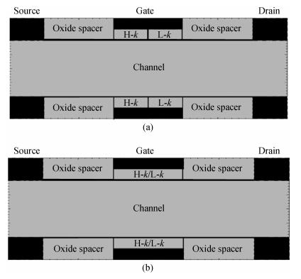
Fig. 1.
A 2-D schematic structure of (a) a HGJLT-dual-k JLT, (b) a double gate junctionless transistor with high-k gate dielectric only (high-k JLT)/low-k gate dielectric only (low-k JLT)
SEMICONDUCTOR DEVICES
Bahniman Ghosh1, 2, Partha Mondal2, M. W. Akram2, Punyasloka Bal2 and Akshay Kumar Salimath2
Corresponding author: Bahniman Ghosh, Email: bghosh@utexas.edu; Akshay Kumar Salimath, Email: salimath@iitk.ac.in
Abstract: We propose a hetero-gate-dielectric double gate junctionless transistor (HGJLT), taking high-k gate insulator at source side and low-k gate insulator at drain side, which reduces the effects of band-to-band tunnelling (BTBT) in the sub-threshold region. A junctionless transistor (JLT) is turned off by the depletion of carriers in the highly doped thin channel (device layer) which results in a significant band overlap between the valence band of the channel region and the conduction band of the drain region, due to off-state drain bias, that triggers electrons to tunnel from the valence band of the channel region to the conduction band of the drain region leaving behind holes in the channel.These effects of band-to-band tunnelling increase the sub-threshold leakage current, and the accumulation of holes in the channel forms a parasitic bipolar junction transistor (n-p-n BJT for channel JLT) in the lateral direction by the source (emitter), channel (base) and drain (collector) regions in JLT structure in off-state. The proposed HGJLT reduces the subthreshold leakage current and suppresses the parasitic BJT action in off-state by reducing the band-to-band tunnelling probability.
Keywords: hetero-gate-dielectric double gate junctionless transistor, band-to-band tunnelling, off-state
| [1] |
Colinge J P, Lee C W, Afzalian A, et al. Nanowire transistors without junctions. Nature Nanotechnol, 2010, 5(3):225 doi: 10.1038/nnano.2010.15
|
| [2] |
Lilienfeld J E. Method and apparatus for controlling electric current. US Patent, No. 1745175, Jan. 28, 1930
|
| [3] |
Chen C, Lin J, Chiang M, et al. High-performance ultra-low power junctionless nanowire FET on SOI substrate in subthreshold logic application. Proc IEEE Int SOI Conf, 2010:1
|
| [4] |
Lee C W, fzalian A, Akhavan N D, et al. Junctionless multigate field-effect transistor. Appl Phys Lett, 2009, 94(5):053511 doi: 10.1063/1.3079411
|
| [5] |
Kranti A, Lee C W, Ferain I, et al. Junctionless nanowire transistor:properties and design guidelines. Proc IEEE 34th Eur Solid-State Device Res Conf, 2010:357
|
| [6] |
Gundapaneni S, Ganguly S, Kottantharayil A. Bulk planar junctionless transistor (BPJLT):an attractive device alternative for scaling. IEEE Electron Device Lett, 2011, 32(3):261 doi: 10.1109/LED.2010.2099204
|
| [7] |
Mondal P, Ghosh B, Bal P. Planar junctionless transistor with non-uniform channel doping. Appl Phys Lett, 2013, 102(13):133505 doi: 10.1063/1.4801443
|
| [8] |
Lee C W, Ferain I, Afzalian A, et al. Performance estimation of junctionless multigate transistors. Solid-State Electron, 2010, 54(2):97 doi: 10.1016/j.sse.2009.12.003
|
| [9] |
Lee C W, Ferain I, Akhavan N D, et al. Short-channel junctionless nanowire transistors. Proc SSDM, 2010:1044
|
| [10] |
Gundapaneni S, Bajaj M, Pandey R K, et al. Effect of band-to-band tunneling on junctionless transistors. IEEE Trans Electron Devices, 2012, 59(4):1023 doi: 10.1109/TED.2012.2185800
|
| [11] |
Ran Y, Das S, Ferain I, et al. Device design and estimated performance for p-type junctionless transistors on bulk germanium substrates. IEEE Trans Electron Devices, 2012, 59(9):2308 doi: 10.1109/TED.2012.2202239
|
| [12] |
Pai C Y, Lin J T, Wang S W, et al. Numerical study of performance comparison between junction and junctionless thin-film transistors. 10th IEEE International Conference on Solid-State and Integrated Circuit Technology (ICSICT), 2010:1410
|
| [13] |
Su T K, Tsai T I, Su C J, et al. Fabrication and characterization of a junctionless SONOS transistor with poly-Si nanowire channels. IEEE 4th International Nanoelectronics Conference (INEC), 2011:1
|
| [14] |
Park C H, Ko M D, Kim K H, et al. Comparative study of fabricated junctionless and inversion-mode nanowire FETs. 69th Annual Device Research Conference (DRC), 2011:179
|
| [15] |
Park C H, Ko M D, Kim K H, et al. Electrical characteristics of 20-nm junctionless Si nanowire transistors. Solid-State Electron, 2012, 73:7 doi: 10.1016/j.sse.2011.11.032
|
| [16] |
Choi W Y, Lee W. Hetero-gate-dielectric tunnelling field-effect transistors. IEEE Trans Electron Devices, 2010, 57(9):2317 doi: 10.1109/TED.2010.2052167
|
| [17] |
Lee M J, Choi W Y. Effects of device geometry on hetero-gate-dielectric tunneling field-effect transistors. IEEE Electron Device Lett, 2012, 33(10):1459 doi: 10.1109/LED.2012.2206790
|
| [18] |
Lee G, Jang J S, Choi W Y. Dual-dielectric-constant spacer hetero-gate-dielectric tunneling field-effect transistors. Semicond Sci Technol, 2013, 28:052001 doi: 10.1088/0268-1242/28/5/052001
|
| [19] |
Ikarashi N, Watanabe K, Masuzaki K, et al. Thermal stability of a HfO2/SiO2 interface. Appl Phys Lett, 2006, 88(10):101912 doi: 10.1063/1.2182023
|
| [20] |
Taurus Medici User Guide Version X-2005. 10, October 2005
|
| [21] |
Boucart K, Ionescu A M. Double-gate tunnel FET with high-k gate dielectric. IEEE Trans Electron Devices, 2007, 54(7):1725 doi: 10.1109/TED.2007.899389
|
| [22] |
International Technology Roadmap for Semiconductors (ITRS), 2011. [Online]. Available: http://www.itrs.net/
|
| [23] |
Appenzeller J, Lin Y M, Knoch J, et al. Band-to-band tunnelling in carbon nanotube field effect transistors. Phys Rev Lett, 2004, 93(19):196
|
| [24] |
Sedra A S, Smith K C. Microelectronic circuits. 6th ed. Oxford University Press, 2009
|
| [25] |
Baruah R K, Paily R P. Impact of high-k spacer on device performance of a junctionless transistor. Journal of Computational Electronics (online), Springer US, 12 Dec 2012. http://dx.doi.org/10.1007/s10825-012-0428-5
|
| [26] |
Gundapaneni S, Ganguly S, Kottantharayil A. Enhanced electrostatic integrity of short-channel junctionless transistor with high-k spacers. IEEE Electron Device Lett, 2011, 32(10):1325 doi: 10.1109/LED.2011.2162309
|
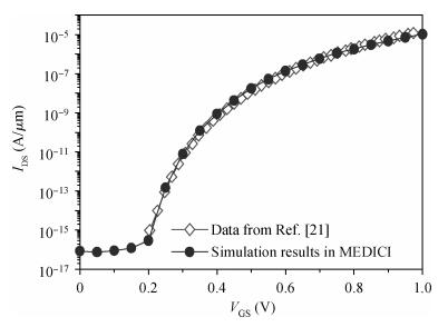
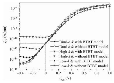
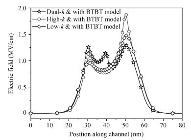
Table 1. Parameters used for the device simulation

|
| [1] |
Colinge J P, Lee C W, Afzalian A, et al. Nanowire transistors without junctions. Nature Nanotechnol, 2010, 5(3):225 doi: 10.1038/nnano.2010.15
|
| [2] |
Lilienfeld J E. Method and apparatus for controlling electric current. US Patent, No. 1745175, Jan. 28, 1930
|
| [3] |
Chen C, Lin J, Chiang M, et al. High-performance ultra-low power junctionless nanowire FET on SOI substrate in subthreshold logic application. Proc IEEE Int SOI Conf, 2010:1
|
| [4] |
Lee C W, fzalian A, Akhavan N D, et al. Junctionless multigate field-effect transistor. Appl Phys Lett, 2009, 94(5):053511 doi: 10.1063/1.3079411
|
| [5] |
Kranti A, Lee C W, Ferain I, et al. Junctionless nanowire transistor:properties and design guidelines. Proc IEEE 34th Eur Solid-State Device Res Conf, 2010:357
|
| [6] |
Gundapaneni S, Ganguly S, Kottantharayil A. Bulk planar junctionless transistor (BPJLT):an attractive device alternative for scaling. IEEE Electron Device Lett, 2011, 32(3):261 doi: 10.1109/LED.2010.2099204
|
| [7] |
Mondal P, Ghosh B, Bal P. Planar junctionless transistor with non-uniform channel doping. Appl Phys Lett, 2013, 102(13):133505 doi: 10.1063/1.4801443
|
| [8] |
Lee C W, Ferain I, Afzalian A, et al. Performance estimation of junctionless multigate transistors. Solid-State Electron, 2010, 54(2):97 doi: 10.1016/j.sse.2009.12.003
|
| [9] |
Lee C W, Ferain I, Akhavan N D, et al. Short-channel junctionless nanowire transistors. Proc SSDM, 2010:1044
|
| [10] |
Gundapaneni S, Bajaj M, Pandey R K, et al. Effect of band-to-band tunneling on junctionless transistors. IEEE Trans Electron Devices, 2012, 59(4):1023 doi: 10.1109/TED.2012.2185800
|
| [11] |
Ran Y, Das S, Ferain I, et al. Device design and estimated performance for p-type junctionless transistors on bulk germanium substrates. IEEE Trans Electron Devices, 2012, 59(9):2308 doi: 10.1109/TED.2012.2202239
|
| [12] |
Pai C Y, Lin J T, Wang S W, et al. Numerical study of performance comparison between junction and junctionless thin-film transistors. 10th IEEE International Conference on Solid-State and Integrated Circuit Technology (ICSICT), 2010:1410
|
| [13] |
Su T K, Tsai T I, Su C J, et al. Fabrication and characterization of a junctionless SONOS transistor with poly-Si nanowire channels. IEEE 4th International Nanoelectronics Conference (INEC), 2011:1
|
| [14] |
Park C H, Ko M D, Kim K H, et al. Comparative study of fabricated junctionless and inversion-mode nanowire FETs. 69th Annual Device Research Conference (DRC), 2011:179
|
| [15] |
Park C H, Ko M D, Kim K H, et al. Electrical characteristics of 20-nm junctionless Si nanowire transistors. Solid-State Electron, 2012, 73:7 doi: 10.1016/j.sse.2011.11.032
|
| [16] |
Choi W Y, Lee W. Hetero-gate-dielectric tunnelling field-effect transistors. IEEE Trans Electron Devices, 2010, 57(9):2317 doi: 10.1109/TED.2010.2052167
|
| [17] |
Lee M J, Choi W Y. Effects of device geometry on hetero-gate-dielectric tunneling field-effect transistors. IEEE Electron Device Lett, 2012, 33(10):1459 doi: 10.1109/LED.2012.2206790
|
| [18] |
Lee G, Jang J S, Choi W Y. Dual-dielectric-constant spacer hetero-gate-dielectric tunneling field-effect transistors. Semicond Sci Technol, 2013, 28:052001 doi: 10.1088/0268-1242/28/5/052001
|
| [19] |
Ikarashi N, Watanabe K, Masuzaki K, et al. Thermal stability of a HfO2/SiO2 interface. Appl Phys Lett, 2006, 88(10):101912 doi: 10.1063/1.2182023
|
| [20] |
Taurus Medici User Guide Version X-2005. 10, October 2005
|
| [21] |
Boucart K, Ionescu A M. Double-gate tunnel FET with high-k gate dielectric. IEEE Trans Electron Devices, 2007, 54(7):1725 doi: 10.1109/TED.2007.899389
|
| [22] |
International Technology Roadmap for Semiconductors (ITRS), 2011. [Online]. Available: http://www.itrs.net/
|
| [23] |
Appenzeller J, Lin Y M, Knoch J, et al. Band-to-band tunnelling in carbon nanotube field effect transistors. Phys Rev Lett, 2004, 93(19):196
|
| [24] |
Sedra A S, Smith K C. Microelectronic circuits. 6th ed. Oxford University Press, 2009
|
| [25] |
Baruah R K, Paily R P. Impact of high-k spacer on device performance of a junctionless transistor. Journal of Computational Electronics (online), Springer US, 12 Dec 2012. http://dx.doi.org/10.1007/s10825-012-0428-5
|
| [26] |
Gundapaneni S, Ganguly S, Kottantharayil A. Enhanced electrostatic integrity of short-channel junctionless transistor with high-k spacers. IEEE Electron Device Lett, 2011, 32(10):1325 doi: 10.1109/LED.2011.2162309
|


Article views: 3376 Times PDF downloads: 29 Times Cited by: 0 Times
Received: 13 November 2013 Revised: Online: Published: 01 June 2014
| Citation: |
Bahniman Ghosh, Partha Mondal, M. W. Akram, Punyasloka Bal, Akshay Kumar Salimath. Hetero-gate-dielectric double gate junctionless transistor (HGJLT) with reduced band-to-band tunnelling effects in subthreshold regime[J]. Journal of Semiconductors, 2014, 35(6): 064001. doi: 10.1088/1674-4926/35/6/064001
****
B Ghosh, P Mondal, M. W. Akram, P Bal, A K Salimath. Hetero-gate-dielectric double gate junctionless transistor (HGJLT) with reduced band-to-band tunnelling effects in subthreshold regime[J]. J. Semicond., 2014, 35(6): 064001. doi: 10.1088/1674-4926/35/6/064001.

|
| [1] |
Colinge J P, Lee C W, Afzalian A, et al. Nanowire transistors without junctions. Nature Nanotechnol, 2010, 5(3):225 doi: 10.1038/nnano.2010.15
|
| [2] |
Lilienfeld J E. Method and apparatus for controlling electric current. US Patent, No. 1745175, Jan. 28, 1930
|
| [3] |
Chen C, Lin J, Chiang M, et al. High-performance ultra-low power junctionless nanowire FET on SOI substrate in subthreshold logic application. Proc IEEE Int SOI Conf, 2010:1
|
| [4] |
Lee C W, fzalian A, Akhavan N D, et al. Junctionless multigate field-effect transistor. Appl Phys Lett, 2009, 94(5):053511 doi: 10.1063/1.3079411
|
| [5] |
Kranti A, Lee C W, Ferain I, et al. Junctionless nanowire transistor:properties and design guidelines. Proc IEEE 34th Eur Solid-State Device Res Conf, 2010:357
|
| [6] |
Gundapaneni S, Ganguly S, Kottantharayil A. Bulk planar junctionless transistor (BPJLT):an attractive device alternative for scaling. IEEE Electron Device Lett, 2011, 32(3):261 doi: 10.1109/LED.2010.2099204
|
| [7] |
Mondal P, Ghosh B, Bal P. Planar junctionless transistor with non-uniform channel doping. Appl Phys Lett, 2013, 102(13):133505 doi: 10.1063/1.4801443
|
| [8] |
Lee C W, Ferain I, Afzalian A, et al. Performance estimation of junctionless multigate transistors. Solid-State Electron, 2010, 54(2):97 doi: 10.1016/j.sse.2009.12.003
|
| [9] |
Lee C W, Ferain I, Akhavan N D, et al. Short-channel junctionless nanowire transistors. Proc SSDM, 2010:1044
|
| [10] |
Gundapaneni S, Bajaj M, Pandey R K, et al. Effect of band-to-band tunneling on junctionless transistors. IEEE Trans Electron Devices, 2012, 59(4):1023 doi: 10.1109/TED.2012.2185800
|
| [11] |
Ran Y, Das S, Ferain I, et al. Device design and estimated performance for p-type junctionless transistors on bulk germanium substrates. IEEE Trans Electron Devices, 2012, 59(9):2308 doi: 10.1109/TED.2012.2202239
|
| [12] |
Pai C Y, Lin J T, Wang S W, et al. Numerical study of performance comparison between junction and junctionless thin-film transistors. 10th IEEE International Conference on Solid-State and Integrated Circuit Technology (ICSICT), 2010:1410
|
| [13] |
Su T K, Tsai T I, Su C J, et al. Fabrication and characterization of a junctionless SONOS transistor with poly-Si nanowire channels. IEEE 4th International Nanoelectronics Conference (INEC), 2011:1
|
| [14] |
Park C H, Ko M D, Kim K H, et al. Comparative study of fabricated junctionless and inversion-mode nanowire FETs. 69th Annual Device Research Conference (DRC), 2011:179
|
| [15] |
Park C H, Ko M D, Kim K H, et al. Electrical characteristics of 20-nm junctionless Si nanowire transistors. Solid-State Electron, 2012, 73:7 doi: 10.1016/j.sse.2011.11.032
|
| [16] |
Choi W Y, Lee W. Hetero-gate-dielectric tunnelling field-effect transistors. IEEE Trans Electron Devices, 2010, 57(9):2317 doi: 10.1109/TED.2010.2052167
|
| [17] |
Lee M J, Choi W Y. Effects of device geometry on hetero-gate-dielectric tunneling field-effect transistors. IEEE Electron Device Lett, 2012, 33(10):1459 doi: 10.1109/LED.2012.2206790
|
| [18] |
Lee G, Jang J S, Choi W Y. Dual-dielectric-constant spacer hetero-gate-dielectric tunneling field-effect transistors. Semicond Sci Technol, 2013, 28:052001 doi: 10.1088/0268-1242/28/5/052001
|
| [19] |
Ikarashi N, Watanabe K, Masuzaki K, et al. Thermal stability of a HfO2/SiO2 interface. Appl Phys Lett, 2006, 88(10):101912 doi: 10.1063/1.2182023
|
| [20] |
Taurus Medici User Guide Version X-2005. 10, October 2005
|
| [21] |
Boucart K, Ionescu A M. Double-gate tunnel FET with high-k gate dielectric. IEEE Trans Electron Devices, 2007, 54(7):1725 doi: 10.1109/TED.2007.899389
|
| [22] |
International Technology Roadmap for Semiconductors (ITRS), 2011. [Online]. Available: http://www.itrs.net/
|
| [23] |
Appenzeller J, Lin Y M, Knoch J, et al. Band-to-band tunnelling in carbon nanotube field effect transistors. Phys Rev Lett, 2004, 93(19):196
|
| [24] |
Sedra A S, Smith K C. Microelectronic circuits. 6th ed. Oxford University Press, 2009
|
| [25] |
Baruah R K, Paily R P. Impact of high-k spacer on device performance of a junctionless transistor. Journal of Computational Electronics (online), Springer US, 12 Dec 2012. http://dx.doi.org/10.1007/s10825-012-0428-5
|
| [26] |
Gundapaneni S, Ganguly S, Kottantharayil A. Enhanced electrostatic integrity of short-channel junctionless transistor with high-k spacers. IEEE Electron Device Lett, 2011, 32(10):1325 doi: 10.1109/LED.2011.2162309
|

 WeChat ID
Journal of Semiconductors © 2017 All Rights Reserved 京ICP备05085259号-2

 DownLoad:

