Fig. 1.
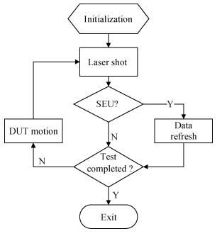
State diagram of SEU sensitivity mapping.
SEMICONDUCTOR DEVICES
Yongtao Yu1, 2, , Guoqiang Feng1, Rui Chen1 and Jianwei Han1
Corresponding author: Yu Yongtao, Email:yuyongtao10@mails.ucas.ac.cn
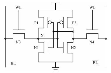
Abstract: The pulsed laser facility for SEU sensitivity mapping is utilized to study the SEU sensitive regions of a 0.18 μm CMOS SRAM cell. Combined with the device layout micrograph, SEU sensitivity maps of the SRAM cell are obtained. TCAD simulation work is performed to examine the SEU sensitivity characteristics of the SRAM cell. The laser mapping experiment results are discussed and compared with the electron micrograph information of the SRAM cell and the TCAD simulation results. The results present that the test technique is reliable and of high mapping precision for the deep submicron technology device.
Keywords: single event upset (SEU), sensitivity mapping, SRAM cell, pulsed laser
| [1] |
Barak J, Adler E, Fischer B E, et al. Microbeam mapping of single event latchups and single event upsets in CMOS SRAMS. IEEE Trans Nucl Sci, 1998, 45(3):1595 doi: 10.1109/23.685246
|
| [2] |
Darracq F, Beauchene T, Pouget V, et al. Single-event sensitivity of a single SRAM cell. IEEE Trans Nucl Sci, 2002, 49(3):1486 doi: 10.1109/TNS.2002.1039688
|
| [3] |
Miller F, Buard N, Hubert G, et al. Laser mapping of SRAM sensitive cells:a way to obtain input parameters for DASIE calculation code. IEEE Trans Nucl Sci, 2006, 53(4):1863 doi: 10.1109/TNS.2006.880938
|
| [4] |
Burnell A J, Chugg A M, Harboe-Sørensen R. Laser SEL sensitivity mapping of SRAM cells. IEEE Trans Nucl Sci, 2010, 57(4):1973 doi: 10.1109/TNS.2009.2039146
|
| [5] |
Chugg A M, Burnell M J, Mourtrie M J, et al. Laser SEE sensitivity mapping of SRAM cells. EEE Trans Nucl Sci, 2007, 54(6):2106 doi: 10.1109/TNS.2007.909514
|
| [6] |
Luo Yinhong, Guo Hongxia, Chen Wei, et al. Laser microbeam experiment on single event effect in SRAM. Microelectronics, 2010, 40(3):464 http://en.cnki.com.cn/Article_en/CJFDTOTAL-MINI201003037.htm
|
| [7] |
Shi Shuting, Guo Gang, Wang Ding, et al. Technique of single event upset mapping. Information and Electronic Engineering, 2012, 10(5):608 http://en.cnki.com.cn/Article_en/CJFDTOTAL-XXYD201205020.htm
|
| [8] |
Feng Guoqiang, Shangguan Shipeng, Ma Yingqi, et al. SEE characteristics of small feature size devices by using laser backside testing. Journal of Semiconductors, 2012, 33(1):014008 doi: 10.1088/1674-4926/33/1/014008
|
| [9] |
Cogenda Pte Ltd, Cogenda TCAD Software, 2011, http://cn.cogenda.com
|
| [10] |
He Chaohui, Li Guozheng, Luo Jinsheng, et al. Analysis of single event upset in CMOS SRAM. Chinese Journal of Semiconductors, 2000, 21(2):174 http://en.cnki.com.cn/Article_en/CJFDTOTAL-BDTX200002012.htm
|
| [11] |
Miller F, Buard N, Carriere T, et al. Effects of beam spot size on the correlation between laser and heavy ion SEU testing. IEEE Trans Nucl Sci, 2004, 51(6):3708 doi: 10.1109/TNS.2004.839261
|

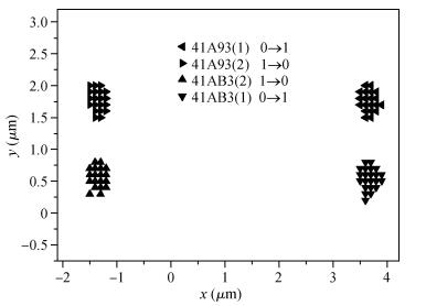
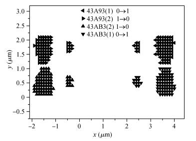
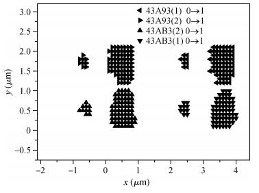
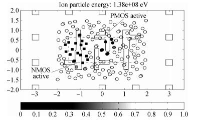
Table 1. Comparison between experiment results and SRAM micrograph.

|
| [1] |
Barak J, Adler E, Fischer B E, et al. Microbeam mapping of single event latchups and single event upsets in CMOS SRAMS. IEEE Trans Nucl Sci, 1998, 45(3):1595 doi: 10.1109/23.685246
|
| [2] |
Darracq F, Beauchene T, Pouget V, et al. Single-event sensitivity of a single SRAM cell. IEEE Trans Nucl Sci, 2002, 49(3):1486 doi: 10.1109/TNS.2002.1039688
|
| [3] |
Miller F, Buard N, Hubert G, et al. Laser mapping of SRAM sensitive cells:a way to obtain input parameters for DASIE calculation code. IEEE Trans Nucl Sci, 2006, 53(4):1863 doi: 10.1109/TNS.2006.880938
|
| [4] |
Burnell A J, Chugg A M, Harboe-Sørensen R. Laser SEL sensitivity mapping of SRAM cells. IEEE Trans Nucl Sci, 2010, 57(4):1973 doi: 10.1109/TNS.2009.2039146
|
| [5] |
Chugg A M, Burnell M J, Mourtrie M J, et al. Laser SEE sensitivity mapping of SRAM cells. EEE Trans Nucl Sci, 2007, 54(6):2106 doi: 10.1109/TNS.2007.909514
|
| [6] |
Luo Yinhong, Guo Hongxia, Chen Wei, et al. Laser microbeam experiment on single event effect in SRAM. Microelectronics, 2010, 40(3):464 http://en.cnki.com.cn/Article_en/CJFDTOTAL-MINI201003037.htm
|
| [7] |
Shi Shuting, Guo Gang, Wang Ding, et al. Technique of single event upset mapping. Information and Electronic Engineering, 2012, 10(5):608 http://en.cnki.com.cn/Article_en/CJFDTOTAL-XXYD201205020.htm
|
| [8] |
Feng Guoqiang, Shangguan Shipeng, Ma Yingqi, et al. SEE characteristics of small feature size devices by using laser backside testing. Journal of Semiconductors, 2012, 33(1):014008 doi: 10.1088/1674-4926/33/1/014008
|
| [9] |
Cogenda Pte Ltd, Cogenda TCAD Software, 2011, http://cn.cogenda.com
|
| [10] |
He Chaohui, Li Guozheng, Luo Jinsheng, et al. Analysis of single event upset in CMOS SRAM. Chinese Journal of Semiconductors, 2000, 21(2):174 http://en.cnki.com.cn/Article_en/CJFDTOTAL-BDTX200002012.htm
|
| [11] |
Miller F, Buard N, Carriere T, et al. Effects of beam spot size on the correlation between laser and heavy ion SEU testing. IEEE Trans Nucl Sci, 2004, 51(6):3708 doi: 10.1109/TNS.2004.839261
|


Article views: 2788 Times PDF downloads: 24 Times Cited by: 0 Times
Received: 05 December 2013 Revised: 12 January 2014 Online: Published: 01 June 2014
| Citation: |
Yongtao Yu, Guoqiang Feng, Rui Chen, Jianwei Han. Laser SEU sensitivity mapping of deep submicron CMOS SRAM[J]. Journal of Semiconductors, 2014, 35(6): 064011. doi: 10.1088/1674-4926/35/6/064011
****
Y T Yu, G Q Feng, R Chen, J W Han. Laser SEU sensitivity mapping of deep submicron CMOS SRAM[J]. J. Semicond., 2014, 35(6): 064011. doi: 10.1088/1674-4926/35/6/064011.

|
| [1] |
Barak J, Adler E, Fischer B E, et al. Microbeam mapping of single event latchups and single event upsets in CMOS SRAMS. IEEE Trans Nucl Sci, 1998, 45(3):1595 doi: 10.1109/23.685246
|
| [2] |
Darracq F, Beauchene T, Pouget V, et al. Single-event sensitivity of a single SRAM cell. IEEE Trans Nucl Sci, 2002, 49(3):1486 doi: 10.1109/TNS.2002.1039688
|
| [3] |
Miller F, Buard N, Hubert G, et al. Laser mapping of SRAM sensitive cells:a way to obtain input parameters for DASIE calculation code. IEEE Trans Nucl Sci, 2006, 53(4):1863 doi: 10.1109/TNS.2006.880938
|
| [4] |
Burnell A J, Chugg A M, Harboe-Sørensen R. Laser SEL sensitivity mapping of SRAM cells. IEEE Trans Nucl Sci, 2010, 57(4):1973 doi: 10.1109/TNS.2009.2039146
|
| [5] |
Chugg A M, Burnell M J, Mourtrie M J, et al. Laser SEE sensitivity mapping of SRAM cells. EEE Trans Nucl Sci, 2007, 54(6):2106 doi: 10.1109/TNS.2007.909514
|
| [6] |
Luo Yinhong, Guo Hongxia, Chen Wei, et al. Laser microbeam experiment on single event effect in SRAM. Microelectronics, 2010, 40(3):464 http://en.cnki.com.cn/Article_en/CJFDTOTAL-MINI201003037.htm
|
| [7] |
Shi Shuting, Guo Gang, Wang Ding, et al. Technique of single event upset mapping. Information and Electronic Engineering, 2012, 10(5):608 http://en.cnki.com.cn/Article_en/CJFDTOTAL-XXYD201205020.htm
|
| [8] |
Feng Guoqiang, Shangguan Shipeng, Ma Yingqi, et al. SEE characteristics of small feature size devices by using laser backside testing. Journal of Semiconductors, 2012, 33(1):014008 doi: 10.1088/1674-4926/33/1/014008
|
| [9] |
Cogenda Pte Ltd, Cogenda TCAD Software, 2011, http://cn.cogenda.com
|
| [10] |
He Chaohui, Li Guozheng, Luo Jinsheng, et al. Analysis of single event upset in CMOS SRAM. Chinese Journal of Semiconductors, 2000, 21(2):174 http://en.cnki.com.cn/Article_en/CJFDTOTAL-BDTX200002012.htm
|
| [11] |
Miller F, Buard N, Carriere T, et al. Effects of beam spot size on the correlation between laser and heavy ion SEU testing. IEEE Trans Nucl Sci, 2004, 51(6):3708 doi: 10.1109/TNS.2004.839261
|

 WeChat ID
Journal of Semiconductors © 2017 All Rights Reserved 京ICP备05085259号-2

 DownLoad: