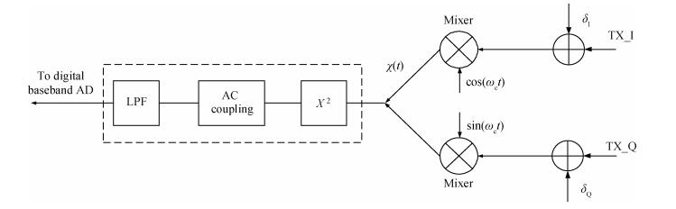
Processing math: 100%
J. Semicond. > 2014, Volume 35 > Issue 6 > 065003

SEMICONDUCTOR INTEGRATED CIRCUITS

A carrier leakage calibration and compensation technique for wideband wireless transceiver

Liguo Zhou1, , Jin Peng1, Fang Yuan1, Zhi Fang2, Jun Yan1 and Yin Shi1

+ Author Affiliations

 Corresponding author: Zhou Liguo, Email:shmilydou@sina.com

DOI: 10.1088/1674-4926/35/6/065003

PDF

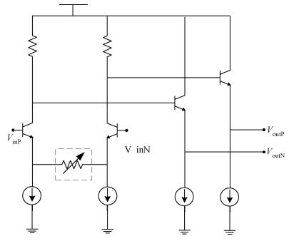
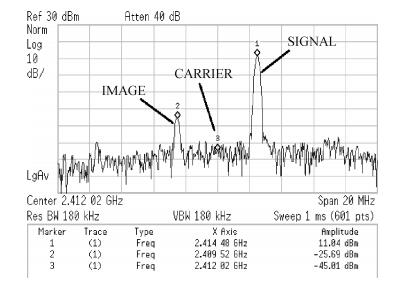
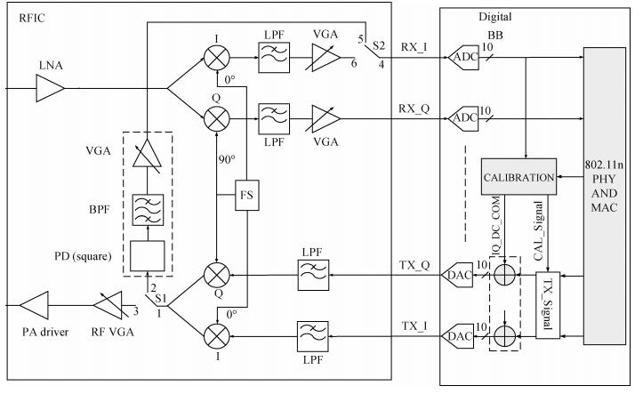
Abstract: A carrier leakage calibration and compensation technique based on digital baseband for a wideband wireless communication transceiver is proposed. The digital baseband transmits a calibration signal, samples the signal which passes through the transmitter path and the calibration loop in the RF chip, measures the carrier leakage by analyzing the sampled data and compensates it. Compared with a self-calibration technique in the RF chip, the proposed technique saves area and power consumption for the wireless local area network (WLAN) solution. This technique has been successfully used for 802.11n system and satisfies the requirement of the standard by achieving over 50 dB carrier leakage suppression.

Key words: 802.11nWLANdirect-conversioncarrier leakagecalibrationDC offset

Silicon carbide (SiC),which exhibits a wider band gap as well as a superior breakdown field and thermal conductivity over conventional Si,has gained considerable attention for a new generation of power devices[1, 2, 3]. However,the metal oxide semiconductor field effect transistors (MOSFETs) fabricated on 4H-SiC present low inversion channel mobility and have a gate oxide reliability problem due to the high density of interface traps at the SiO2/SiC interface[4, 5, 6]. The nitridation process that nitrogen is incorporated into the SiO2/SiC interface,is considered to play a major role in defect passivation[6, 7, 8]. More recently,new routes to improve channel performance have also been proposed,including alkali and alkaline earth elements passivation[9]. Although other processes such as wet oxidation[10],sodium-contaminated oxidation[11, 12],or POCl3 annealing[13, 14] also improve the mobility,nitridation is the most common process,taking reliability and stability into consideration. It lowers the DIT and increases the field effect mobility from 5 to 30 cm2/(Vs),which makes the commercialization of SiC MOSFETs a reality. However,the peak electron inversion-layer mobility at moderate doping levels is expected to be 200 cm2/(Vs) or higher,considering the SiC bulk electron mobility of 954 cm2/(Vs)[15, 16] }.Asthedevelopmentofthecharacterizationtechnique,theproblemsofthenitridationprocessaregraduallyrevealed.LargefrequencydispersionisobservedbylowtemperatureCV$ measurements[17]. It is indicated that very fast states still exist at the SiO2/SiC interface even after NO annealing. The traditional high-low method with a maximum frequency of 1 MHz will seriously underestimate the DIT[18]. These conclusions are further confirmed by Kimoto's group,and they find that only a part of the fast states can be detected by conductance measurements up to 100 MHz at room temperature[19]. They also propose a C-ψS method to accurately evaluate the DIT at the SiO2/SiC interface[20]. Recently,a low temperature conductance method,which is supposed to be more suitable for characterization of very fast interface states at the nitrided interface,has been used to study the effects of the fast interface states[21]. Yoshioka reports that the capture cross section of these fast states is uniquely larger than that of conventional interface states and the density of these fast states also increases with NO temperature.

Carbon related defects have been found at the SiO2/SiC interface[8, 22, 23]. Physical defects that are attributed to the high DIT are carbon clusters,C dangling bonds and a nonstoichiometric sub-oxide near the interface[24, 25, 26]. It is suggested that NO annealing can dissolve interfacial carbon clusters,which leads to a reduction of the size of these clusters and possibly generates carbon dangling bonds at the interface[8, 27, 28]. In addition,since the nitridation process is usually performed at a temperature as high as 1350 \du,sub-oxide generation may become non-negligible during the high temperature process[29, 30]. Hydrogen passivation treatment (forming gas annealing: FGA) is routinely applied for Si-based MOS devices. Theoretical studies show that H2 can passivate isolated C dangling bonds as well as Si related defects[31]. It has been shown that nitrogen plasma exposure promotes hydrogen passivation of electrical defects at the SiO2/SiC interface[32].

In this article,we propose a treatment that combines NO annealing and FGA treatment to improve the electrical properties of the SiO2/SiC interface further. The role of nitrogen and hydrogen passivation on the SiO2/4H-SiC interface is evaluated by low-temperature conductance measurements.

MOS capacitors were used to characterize the effects of the passivation treatments on the interface of SiO2/SiC. Figure 1 represents the structure of the SiC MOS capacitor and its fabrication process flow. The starting substrate was an n-type 4H-SiC (0001) wafer with a 12 μm epilayer (ND 4.4 × 1015 cm3). After standard RCA cleaning,45-nm-thick oxides were formed by dry oxidation at 1300 \du,followed by post-oxidation annealing at 1300 \du in N2. Film thickness was determined by UVISEL spectroscopic ellipsometry[33]. Nitridation was carried out in NO (sample label: NO) at 1300 \du for 120 min. During the nitridation,an extra oxide growth took place and the thickness of SiO2 was about 61 nm. FGA annealing was performed in forming gas (5% H2 + 95% N2) ambient (sample label: FGA). For the combined treatment (sample label: NO & FGA),the NO & FGA sample first underwent nitridation and was then annealed in forming gas. A control sample without NO annealing or FG annealing was also prepared (sample label: as-oxidized). Circular Al electrodes (gate) with a diameter of 200 μm were deposited on the sample surface by a lift-off process.

Figure  图 1.  4H-SiC MOS capacitor and its fabrication process flow. The post-oxidation treatments for each sample are also shown.
Fig.1.

The room temperature conductance measurements were measured at probe frequencies from 1 kHz to 1 MHz using a precision impedance analyzer (4284A,Agilent Technologies). For the NO sample and the NO & FGA sample,low temperature conductance measurements were also carried out at temperatures ranging from 150 to 293 K with a step of 30 K to characterize the fast states. Figure 2 shows the typical parallel-model capacitance (CP) and conductance (GP) for the MOS capacitors.

Figure  Fig2.  (Color online) (a) Typical capacitance–voltage and (b) conductance–voltage characteristics of the MOS capacitors measured at different frequencies (parallel mode).

Based on an equivalent circuit shown in Figure 3,the interface state conductance (GPIT) was extracted from the measured impedance. Before applying the conductance method,the values of the Z(ω) were determined for each frequency from the impedance and Cox measured in a strong accumulation region. Then,series resistance was removed from the measured impedance[34]. The interface state density is linked to GPIT by[35]

Figure  Fig3.  Equivalent circuit for a MOS capacitor, where Cox, CD, CIT, and GPIT are the oxide capacitance, the semiconductor capacitance, the interface-state capacitance, and the interface-state conductance, respectively.

where ω is the angular frequency,S is the area of the gate electrode,and e (1.602 × 10¹⁹ C) is the elementary electric charge. The interface state density (DIT),the time constant of the interface states (τ),and the standard deviation (σ) are determined using a simple method provided by Nicollian and Brews[35]. The energy level (Ec - ET) of interface states is calculated from

by taking into account the Fermi level of the SiC epilayer (Ec - 0.24 eV) at room temperature. Here ψs is the surface potential determined from a comparison of an ideal C-V curve and the measured high frequency C-V curve. For the low temperature measurements,the incomplete dopant ionization effect in 4H-SiC is also taken into consideration when calculating the Fermi level[36]. The stability of the flatband voltage was also evaluated by C-V measurements.

The C-V characteristics measured with various frequencies from 1 kHz to 1 MHz for the MOS capacitors are shown in Figure 4. Both the as-deposited sample and the FGA sample show large frequency dispersion,which indicates the formation of an interface with a high density of interface defects. As for the NO sample and the NO & FGA sample,the C-V curves agree well with each other. Figure 5 shows interface-state conductances (GPIT) at different gate voltages for these samples. A broad single peak is observed for the as-oxidized sample and FGA sample,which is consistent with C-V results. From the peaks,DIT values of the as-oxidized sample and FGA sample are determined at each gate voltage and shown in Figure 6(a) as a function of the energy level with reference to the conduction band edge of SiC. H2 has only a limited effect on the DIT,which is accorded with earlier reports[37]. Two reasons may account for this result. Firstly,H2 can passivate Si dangling bonds and isolated C dangling bonds,but these kinds of defects are not the dominant defects in the as-oxidized SiO2/SiC interface. Secondly,H2 has a large diffusion barrier (> 2.5 eV) in SiO2 and needs a relatively high annealing temperature[38]. Although FGA treatment has a small effect on the DIT,the values of time constant (τ) show a significant decrease compared with the as-oxidized sample,especially at a trap energy level close to the conduction band edge of SiC.

Figure  Fig4.  The parallel-mode capacitance measured at different frequencies for SiC-MOS capacitors underwent various fabrication conditions. The measurements are performed at room temperature.
Figure  Fig5.  Interface-state conductance against frequency for SiC-MOS capacitors under various fabrication conditions. The measurements are performed at room temperature.
Figure  Fig6.  (a) The densities of interface states and (b) time constant for the as-oxidized sample and FGA sample. The values were extracted from conductance measurements at room temperature.

As shown in Figure 5,the NO sample and NO & FGA sample do not show any peaks throughout the measurable frequency range because these peaks take a maximum frequency higher than 1 MHz. However,it does not mean that there is a low density of interface states in these samples. It has been reported that the density of conventional states existing at an as-oxidized interface decreases significantly after NO annealing and new defects with a very fast time constant are observed[19]. These fast interface states can respond to frequencies higher than 100 MHz at room temperature (RT),so it needs an ultra-high frequency measurement or other measurement approach. Since the response frequency of fast states is lowered with decreasing temperature,the DIT is evaluated by low temperature conductance measurements for the NO sample and NO & FGA sample.

Here the impedance-frequency characteristics are measured in a temperature range of T= 150 - 298 K and the peaks of GPIT are only found in a range of T 210 K. Figure 7 shows the parallel-mode capacitance measured at low temperatures (210 K/180 K/150 K) for the NO & FGA sample. The frequency dispersion increases obviously with reducing the measurement temperature. Since the response frequency of interface states is lowered with decreasing temperature,for T < 210 K,1 MHz is almost high enough for the GPIT peak to be clearly observed. Figure 8 shows the GPIT at different gate voltages for the NO & FGA sample. Distinct peaks are observed for both the samples. The DIT of all the samples is then summarized in Figure 9. The detectable energy level is as shallow as 0.1 eV by low temperature measurements. Even though the DIT decreases obviously after NO annealing,the interface states density is still more than 1012 cm2 eV1 at shallower than 0.2 eV. The values of DIT are reasonable compared with earlier reports[21]. As for the NO & FGA sample,the DIT is further reduced after additional FG annealing. Though FG annealing has a limited effect on the shallow traps,deeper in the energy bandgap (EC - ET 0.4 eV),the DIT is reduced to less than 1011 cm2 eV1.

Figure  Fig7.  The parallel-mode capacitance for the NO & FGA sample measured at low temperatures.
Figure  Fig8.  Interface-state conductance against frequency for the NO & FGA sample measured at low temperatures.
Figure  Fig9.  The density of interface-states for SiC-MOS capacitors under various fabrication conditions.

As shown in Figure 9,FGA treatment at 450 \du alone does not have any impact improvement of the electrical properties. It is well known that Si-O-C bonds and C-C clusters,as well as C dangling bonds are supposed to be the possible origins of interface states in SiC-MOS devices. However,the Nitridation process can dissolve carbon clusters and associated complex Si-O-C bonds,which leads to the formation of simple Si and C dangling bonds that can be readily terminated by H2. Thus,the density of interface states (EC - ET 0.2 eV) decreases dramatically after a treatment combining NO and forming gas annealing. This result is consistent with the theoretical study that carbon-related defects can explain most of the observed interface states but not the high density near the conduction band of 4H-SiC[39]. Figure 10 shows the interface-state conductance against temperature for the NO & FGA sample measured at 100 kHz. Multiple lines show the results measured at different gate voltages. The conventional interface-state conductance peak,which usually exists at the as-oxidized SiO2/SiC interface and responds at room temperature,is effectively suppressed. The fast interface-state conductance peak is larger than the conventional interface-state conductance peak and is located at lower temperature in T-sweep measurements at 100 kHz. As for these fast interface states,we can rule out the possibility that simple Si dangling bonds and C dangling bonds,which were easy to be terminated with H2,are the dominant component of these traps. Yoshioka reports that the density of fast states increases almost in proportion to the N concentration at the SiO2/SiC interface[21]. Distinct N peaks are also found for both the NO sample and the NO & FGA sample in XPS measurements as shown in Figure 11. N atoms accumulated at the interface by the process are considered as a possible origin of these shallow traps (EC - ET 0.2 eV).

Figure  Fig10.  Interface-state conductance against temperature for the NO & FGA sample measured at 100 kHz. Multiple lines show the results measured at different gate voltages.
Figure  Fig11.  XPS spectra of N 1s for the SiO2/SiC structures under various fabrication conditions.

The stability of VFB against the accumulation voltage is investigated at room temperature. All the C-V sweeps (1 MHz) are started from -5 V,and the maximum accumulation voltage (Vacc) is varied from 10 to 24 V with a 2-V step. The flatband voltage shifts corresponding to these C-V curves are summarized in Figure 12. Significant positive VFB shifts are observed for the as-deposited sample and FGA sample. Positive shifts occur when the acceptor-like deep interface states are filled with electrons under a strong accumulation region. Most of them are difficult to detrap and act like negative fixed charges. Thus,a positive shift of the C-V curves is observed. The VFB shift almost disappears for the NO & FGA sample. This is because the DIT of the NO & FGA sample decreases by over an order of magnitude compared to that of the as-oxidized sample and especially at the deep energy level. It is indicated that the combined treatment of NO annealing and forming gas annealing is quite effective to suppress the VFB shift for the SiC-MOS devices.

Figure  Fig12.  Flatband voltage shift extracted from C–V characteristics as a function of the maximum accumulation voltage of C–V sweep.

We investigate the role of nitrogen and hydrogen incorporation into the SiO2/SiC interface by conductance measurements. Even though the DIT is significantly reduced in the entire energy range after NO annealing,very fast states are observed at the nitride SiO2/SiC interface and respond to frequencies higher than 1 MHz at room temperature. Through low-temperature conductance measurements,the conductance peak of the NO-annealed capacitor is clearly observed. Forming gas annealing alone is not effective for reducing interface defects,but hydrogen can terminate the residual Si and C dangling bonds generated after NO annealing and the DIT is further reduced. The combined treatment of NO and forming gas annealing reduces the density of interface states in the deep energy trap level to less than 1011 cm2 eV1. The stability of VFB is also remarkably improved due to the reduction of DIT. It is indicated that combined treatment using the nitridation process in conjunction with hydrogen passivation is a promising method for improving the performance of SiC-based MOS devices.


[1]
Zhang P, Der L. A single-chip dual-band direct-conversion IEEE 802.11 a/b/g WLAN transceiver in 0.13-μm CMOS. IEEE J Solid-State circuits, 2005, 40(9):1932 doi: 10.1109/JSSC.2005.848182
[2]
Brenna G, Tschopp D. A 2-GHz carrier leakage calibrated direct-conversion WCDMA transmitter in 0.13-μm CMOS. IEEE J Solid-State circuits, 2004, 39(8):1253 doi: 10.1109/JSSC.2004.831794
[3]
Maas S A. Microwave mixers. 2nd ed. Artech House, 1993
[4]
Minarik R. Circuit for canceling local oscillator leakage through mixers. Microwave Journal, 1985:182 http://www.freepatentsonline.com/5001773.html
[5]
Wang Y, Shou L. A LO-leakage auto-calibration CMOS IEEE802.11b/g WLAN transceiver. IEEE International Symposium on Circuits and Systems, 2007:3912 http://ieeexplore.ieee.org/xpl/articleDetails.jsp?reload=true&arnumber=4253537
[6]
Lanschutzer C, Springer A. Integrated adaptive LO leakage cancellation for W-CDMA direct upconversion transceivers. IEEE Radio Frequency Integrated Circuits (RFIC) Symposium, 2003:19 http://ieeexplore.ieee.org/xpls/icp.jsp?arnumber=1213884
[7]
Fang Yuan. A direct-conversion WLAN transceiver baseband with DC offset compensation and carrier leakage reduction. Journals of Semiconductors, 2010, 31(10):105003 doi: 10.1088/1674-4926/31/10/105003
[8]
Wireless LAN Medium Access Control (MAC) and Physical Layer (PHY) Specifications, Amendment 5: Enhancements for Higher Throughput. New York: The Institute of Electrical and Electronics Engineers, Inc, 2009
Fig. 1.  The transceiver with carrier leakage calibration based on digital baseband.

Fig. 2.  The mathematical model of the calibration system.

Fig. 3.  Calibration procedure of channel I DC offset.

Fig. 4.  The carrier leakage compensation circuits.

Fig. 5.  Schematic of square power detector.

Fig. 6.  Pass-band filter.

Fig. 7.  Low frequency VGA.

Fig. 8.  Die photograph of calibration loop.

Fig. 9.  TX performance of single-sideband signal in low power (4.75 dBm).

Fig. 10.  TX performance of single-sideband signal in high power (10.88 dBm).

Fig. 11.  IEEE 802.11n transmitted signal spectrum.

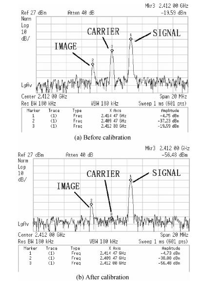
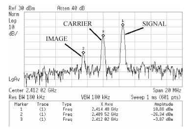
Table 1.   Comparison results of two calibration techniques.

[1]
Zhang P, Der L. A single-chip dual-band direct-conversion IEEE 802.11 a/b/g WLAN transceiver in 0.13-μm CMOS. IEEE J Solid-State circuits, 2005, 40(9):1932 doi: 10.1109/JSSC.2005.848182
[2]
Brenna G, Tschopp D. A 2-GHz carrier leakage calibrated direct-conversion WCDMA transmitter in 0.13-μm CMOS. IEEE J Solid-State circuits, 2004, 39(8):1253 doi: 10.1109/JSSC.2004.831794
[3]
Maas S A. Microwave mixers. 2nd ed. Artech House, 1993
[4]
Minarik R. Circuit for canceling local oscillator leakage through mixers. Microwave Journal, 1985:182 http://www.freepatentsonline.com/5001773.html
[5]
Wang Y, Shou L. A LO-leakage auto-calibration CMOS IEEE802.11b/g WLAN transceiver. IEEE International Symposium on Circuits and Systems, 2007:3912 http://ieeexplore.ieee.org/xpl/articleDetails.jsp?reload=true&arnumber=4253537
[6]
Lanschutzer C, Springer A. Integrated adaptive LO leakage cancellation for W-CDMA direct upconversion transceivers. IEEE Radio Frequency Integrated Circuits (RFIC) Symposium, 2003:19 http://ieeexplore.ieee.org/xpls/icp.jsp?arnumber=1213884
[7]
Fang Yuan. A direct-conversion WLAN transceiver baseband with DC offset compensation and carrier leakage reduction. Journals of Semiconductors, 2010, 31(10):105003 doi: 10.1088/1674-4926/31/10/105003
[8]
Wireless LAN Medium Access Control (MAC) and Physical Layer (PHY) Specifications, Amendment 5: Enhancements for Higher Throughput. New York: The Institute of Electrical and Electronics Engineers, Inc, 2009
1

A highly linear power amplifier for WLAN

Jie Jin, Jia Shi, Baoli Ai, Xuguang Zhang

Journal of Semiconductors, 2016, 37(2): 025006. doi: 10.1088/1674-4926/37/2/025006

2

An IQ mismatch calibration and compensation technique for wideband wireless transceivers

Jin Peng, Liguo Zhou, Heng Yao, Fang Yuan, Zhi Fang, et al.

Journal of Semiconductors, 2014, 35(8): 085003. doi: 10.1088/1674-4926/35/8/085003

3

VLSI implementation of MIMO detection for 802.11n using a novel adaptive tree search algorithm

Heng Yao, Haifang Jian, Liguo Zhou, Yin Shi

Journal of Semiconductors, 2013, 34(10): 105005. doi: 10.1088/1674-4926/34/10/105005

4

A programmable gain amplifier with digitally assisted DC offset calibration for a direct-conversion WLAN receiver

Yao Xiaocheng, Gong Zheng, Shi Yin

Journal of Semiconductors, 2012, 33(11): 115006. doi: 10.1088/1674-4926/33/11/115006

5

An optimized analog to digital converter for WLAN analog front end

Ye Mao, Zhou Yumei, Wu Bin, Jiang Jianhua

Journal of Semiconductors, 2012, 33(4): 045008. doi: 10.1088/1674-4926/33/4/045008

6

CMOS analog baseband circuitry for an IEEE 802.11 b/g/n WLAN transceiver

Gong Zheng, Chu Xiaojie, Lei Qianqian, Lin Min, Shi Yin, et al.

Journal of Semiconductors, 2012, 33(11): 115001. doi: 10.1088/1674-4926/33/11/115001

7

30-GHz millimeter-wave carrier generation with single sideband modulation based on stimulated Brillouin scattering

Luo Zhen'ao, Xie Liang, Qi Xiaoqiong, Wang Hui

Journal of Semiconductors, 2011, 32(9): 092004. doi: 10.1088/1674-4926/32/9/092004

8

A fully integrated direct-conversion digital satellite tuner in 0.18 μm CMOS

Chen Si, Yang Zengwang, Gu Mingliang

Journal of Semiconductors, 2011, 32(4): 045004. doi: 10.1088/1674-4926/32/4/045004

9

CMOS linear-in-dB VGA with DC offset cancellation for direct-conversion receivers

Lei Qianqian, Chen Zhiming, Shi Yin, Chu Xiaojie, Gong Zheng, et al.

Journal of Semiconductors, 2011, 32(10): 105008. doi: 10.1088/1674-4926/32/10/105008

10

A programmable gain amplifier with a DC offset calibration loop for a direct-conversion WLAN transceiver

Lei Qianqian, Lin Min, Chen Zhiming, Shi Yin

Journal of Semiconductors, 2011, 32(4): 045006. doi: 10.1088/1674-4926/32/4/045006

11

Improved low-distortion sigma–delta ADC with DWA for WLAN standards

Li Di, Yang Yintang, Zhu Zhangming, Shi Lichun, Wu Xiaofeng, et al.

Journal of Semiconductors, 2010, 31(2): 025011. doi: 10.1088/1674-4926/31/2/025011

12

A direct-conversion WLAN transceiver baseband with DC offset compensation and carrier leakage reduction

Yuan Fang, Yan Jun, Ma Heping, Shi Yin, Dai Fa Foster, et al.

Journal of Semiconductors, 2010, 31(10): 105003. doi: 10.1088/1674-4926/31/10/105003

13

5.2 GHz variable-gain amplifier and power amplifier driver for WLAN IEEE 802.11a transmitter front-end

Zhang Xuelian, Yan Jun, Shi Yin, Dai Fa Foster

Journal of Semiconductors, 2009, 30(1): 015008. doi: 10.1088/1674-4926/30/1/015008

14

A VCO sub-band selection circuit for fast PLL calibration

Song Ying, Wang Yuan, Jia Song, Zhao Baoying

Journal of Semiconductors, 2009, 30(8): 085010. doi: 10.1088/1674-4926/30/8/085010

15

A Fully Integrated Low Power Transmitter in an 802.11bTransceiver System

Xia Lingli, Li Weinan, Zheng Yongzheng, Huang Yumei, Hong Zhiliang, et al.

Journal of Semiconductors, 2008, 29(9): 1753-1757.

16

Key Techniques of Frequency Synthesizer for WLAN Receivers

Tang Lu, Wang Zhigong, Xu Yong, Li Zhiqun

Chinese Journal of Semiconductors , 2007, 28(4): 542-548.

17

A Novel Offset-Cancellation Technique for Low Voltage CMOS Differential Amplifiers

Han Shuguang, Chi Baoyong, Wang Zhihua

Chinese Journal of Semiconductors , 2006, 27(5): 778-782.

18

Design of a Monolithic CMOS LC-Voltage Controlled Oscillator with Low Phase Noise for 4GHz Frequency Synthesizers

Tang Lu, Wang Zhigong, Huang Ting, Li Zhiqun

Chinese Journal of Semiconductors , 2006, 27(3): 459-466.

19

A DC-Offset Cancellation Scheme in a Direct-Conversion Receiver for IEEE 802.11a WLAN

Xu Qiming, Shi Yin, Gao Peng, Hu Xueqing, Yan Jun, et al.

Chinese Journal of Semiconductors , 2006, 27(4): 653-657.

20

Simulation of a Monolithic Integrated CMOS Preamplifier for Neural Recordings

Sui Xiaohong, Liu Jinbin, Gu Ming, Pei Weihua, Chen Hongda, et al.

Chinese Journal of Semiconductors , 2005, 26(12): 2275-2280.

  • Search

    Advanced Search >>

    GET CITATION

    Liguo Zhou, Jin Peng, Fang Yuan, Zhi Fang, Jun Yan, Yin Shi. A carrier leakage calibration and compensation technique for wideband wireless transceiver[J]. Journal of Semiconductors, 2014, 35(6): 065003. doi: 10.1088/1674-4926/35/6/065003
    L G Zhou, J Peng, F Yuan, Z Fang, J Yan, Y Shi. A carrier leakage calibration and compensation technique for wideband wireless transceiver[J]. J. Semicond., 2014, 35(6): 065003. doi: 10.1088/1674-4926/35/6/065003.
    shu

    Export: BibTex EndNote

    Article Metrics

    Article views: 4131 Times PDF downloads: 84 Times Cited by: 0 Times

    History

    Received: 19 November 2013 Revised: 08 February 2014 Online: Published: 01 June 2014

    Catalog

      Email This Article

      User name:
      Email:*请输入正确邮箱
      Code:*验证码错误
      Liguo Zhou, Jin Peng, Fang Yuan, Zhi Fang, Jun Yan, Yin Shi. A carrier leakage calibration and compensation technique for wideband wireless transceiver[J]. Journal of Semiconductors, 2014, 35(6): 065003. doi: 10.1088/1674-4926/35/6/065003 ****L G Zhou, J Peng, F Yuan, Z Fang, J Yan, Y Shi. A carrier leakage calibration and compensation technique for wideband wireless transceiver[J]. J. Semicond., 2014, 35(6): 065003. doi: 10.1088/1674-4926/35/6/065003.
      Citation:
      Liguo Zhou, Jin Peng, Fang Yuan, Zhi Fang, Jun Yan, Yin Shi. A carrier leakage calibration and compensation technique for wideband wireless transceiver[J]. Journal of Semiconductors, 2014, 35(6): 065003. doi: 10.1088/1674-4926/35/6/065003 ****
      L G Zhou, J Peng, F Yuan, Z Fang, J Yan, Y Shi. A carrier leakage calibration and compensation technique for wideband wireless transceiver[J]. J. Semicond., 2014, 35(6): 065003. doi: 10.1088/1674-4926/35/6/065003.

      A carrier leakage calibration and compensation technique for wideband wireless transceiver

      DOI: 10.1088/1674-4926/35/6/065003
      More Information
      • Corresponding author: Zhou Liguo, Email:shmilydou@sina.com
      • Received Date: 2013-11-19
      • Revised Date: 2014-02-08
      • Published Date: 2014-06-01

      Catalog

        /

        DownLoad:  Full-Size Img  PowerPoint
        Return
        Return