Fig. 1.
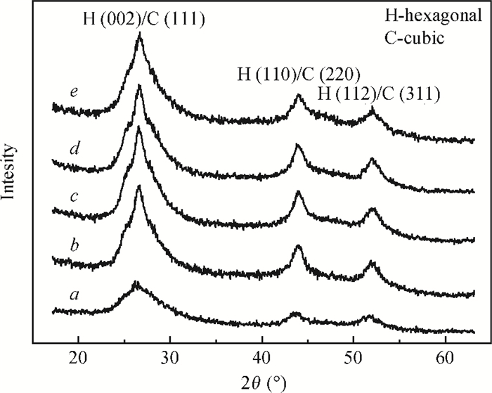
X-ray diffraction patterns of CdS thin films grown at different temperatures. $a$ : 120 ℃. $b$ : 140 ℃. $c$ : 160 ℃. $d$ : 180 ℃. $e$ : 200 ℃.
SEMICONDUCTOR MATERIALS
Fengzhang Zhang1, Xiangqi Li1, Xiaofeng Wu1, Ximei Fan1, and Chaoliang Zhang2
Corresponding author: Fan Ximei, Email:xmfan@home.swjtu.edu.cn
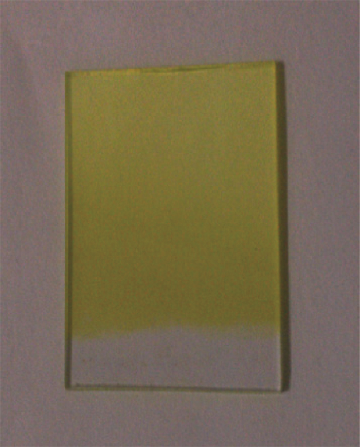
Abstract: CdS thin films were successfully deposited onto glass substrates for the first time by the polyol method using cadmium acetate, thiourea and diethylene glycol as the raw materials. The effects of the deposition temperature from 120 to 200℃ in steps of 20℃ on the structure, morphology and optical properties of the resultant films were investigated. It was found that the crystallinity was improved and the value of the surface average roughness was decreased with increasing the deposition temperature. The average grain sizes of the CdS thin films were 77.16 and 76.61 nm at 140 and 180℃, respectively. All samples showed excellent transmittance and the band gaps were found to reduce from 2.55 to 2.45 eV with the increase of the deposition temperature, which was attributed to the improvement of crystallinity.
Keywords: CdS film, polyol method, deposition temperature, microstructure, optical properties
| [1] |
Li Wei, Feng Lianghuan, Cai Yaping, et al. Microstructure and properties of CdS polycrystalline thin films for solar cells. Chinese Journal of Semiconductors, 2005, 26(1):46 https://www.researchgate.net/publication/286013876_Microstructure_and_properties_of_CdS_polycrystalline_thin_films_for_solar_cells?ev=auth_pub
|
| [2] |
Senthil K, Mangalaraj D, Narayandass S K, et al. Argon and nitrogen implantation effects on the structural and optical properties of vacuum evaporated cadmium sulphide thin films. Semicond Sci Technol, 2002, 17(2):97 doi: 10.1088/0268-1242/17/2/302
|
| [3] |
Seo H K, Ok E A, Kim W M, et al. Electrical and optical characterization of the influence of chemical bath deposition time and temperature on CdS/Cu(In, Ga)Se2 junction properties in Cu(In, Ga)Se2 solar cells. Thin Solid Films, 2013, 546(1):289 http://www.sciencedirect.com/science/article/pii/S0040609013008390
|
| [4] |
Kosyachenko L A, Mathew X, Roshko V Y, et al. Optical absorptivity and recombination losses:The limitations imposed by the thickness of absorber layer in CdS/CdTe solar cells. Solar Energy Materials & Solar Cells, 2013, 114:179 http://www.sciencedirect.com/science/article/pii/S0927024813001165
|
| [5] |
Wang X, Yan X, Li W, et al. Doped quantum dots for white-light-emitting diodes without reabsorption of multiphase phosphors. Adv Mater, 2012, 24(20):2742 doi: 10.1002/adma.v24.20
|
| [6] |
Lin K, Tseng S, Chen H, et al. Ultrahigh-sensitivity CdS photoconductors with instant response and ultralow power consumption for detection in low-light environments. J Mater Chem C, 2013, 1(27):4244 doi: 10.1039/c3tc30520a
|
| [7] |
Lallan Y, Ritesh V, Dwivedi R. Sensing properties of CdS-doped tin oxide thick film gas sensor. Sensors and Actuators B, 2010, 144(1):37 doi: 10.1016/j.snb.2009.10.013
|
| [8] |
Raut B T, Godse P R, Pawar S G, et al. Novel method for fabrication of polyaniline-CdS sensor for H2S gas detection. Measurement, 2012, 45(1):94 doi: 10.1016/j.measurement.2011.09.015
|
| [9] |
Jia H, Hu Y, Tang Y, et al. Synthesis and photoelectrochemical behavior of nanocrystalline CdS film electrodes. Electrochemy Commun, 2006, 8(8):1381 doi: 10.1016/j.elecom.2006.06.025
|
| [10] |
Moualkia H, Hariech S, Aida M S. Structural and optical properties of CdS thin films grown by chemical bath deposition. Thin Solid Films, 2009, 518(4):1259 doi: 10.1016/j.tsf.2009.04.067
|
| [11] |
Liu F, Lai Y, Liu J, et al. Characterization of chemical bath deposited CdS thin films at different deposition temperature. Journal of Alloys and Compounds, 2010, 493(1):305 http://www.sciencedirect.com/science/article/pii/S0925838809026413
|
| [12] |
Ao Jianping, He Qing, Sun Guozhong, et al. Crystal structure and properties of chemical bath deposited CdS thin films. Chinese Journal of Semiconductors, 2005, 26(7):1347 http://en.cnki.com.cn/article_en/cjfdtotal-bdtx200507011.htm
|
| [13] |
Anil M P, Pranaya V J, Vedavati P, et al. Synthesis and X-ray single crystal structure of a cadmium(Ⅱ) acetophenone thiosemicarbazone complex and its use as a single-source precursor for the preparation of CdS nanocrystallites and thin films. Polyhedron, 2013, 61:195 doi: 10.1016/j.poly.2013.05.052
|
| [14] |
Kamila Z, Magdalena S. Electrodeposition of CdS from acidic aqueous thiosulfate solution-investigation of the mechanism by electrochemical quartz microbalance technique. Electrochimica Acta, 2011, 56(16):5731 doi: 10.1016/j.electacta.2011.04.046
|
| [15] |
Boieriu P, Sporken R, Adriaens A, et al. SIMS and XPS characterization of CdS/CdTe heterostructures grown by MBE. Nuclear Instruments and Methods in Physics Research B, 2000, 161-163:975 doi: 10.1016/S0168-583X(99)00926-X
|
| [16] |
Dhawale D S, Duba D P, Phadatare M R, et al. Synthesis and characterizations of CdS nanorods by SILAR method:effect of film thickness. J Mater Sci, 2011, 46(14):5009 doi: 10.1007/s10853-011-5421-z
|
| [17] |
Zhu G, Lv T, Pan L, et al. All spray pyrolysis deposited CdS sensitized ZnO films for quantum dot-sensitized solar cells. Journal of Alloys and Compounds, 2011, 509(2):362 doi: 10.1016/j.jallcom.2010.09.026
|
| [18] |
Feldmann C, Christof M. Polyol mediated synthesis of nanoscale MS particles (M = Zn, Cd, Hg). J Mater Chem, 2001, 11(10):2603 doi: 10.1039/b103167h
|
| [19] |
Quan Z, Li C, Zhang X, et al. Polyol-mediated synthesis of PbS crystals:Shape evolution and growth mechanism. Crystal Growth & Design, 2008, 8(7):2384 http://d.wanfangdata.com.cn/Periodical_NSTL_QKJJ028353061.aspx
|
| [20] |
Sorachon Y, Craig A G. Self-assembled TiO2 nanotube arrays by anodization of titanium in diethylene glycol:approach to extended pore pidening. Langmuir, 2010, 26(1):417 doi: 10.1021/la9020146
|
| [21] |
Feldmann C. Polyol-mediated synthesis of nanoscale functional materials. Adv Funct Mater, 2003, 13(2):101 doi: 10.1002/adfm.v13:2
|
| [22] |
Kurihara L K, Chow G M, Schoen P E. Nanocrystalline metallic powders and films produced by the polyol method. Nanostructured Materials, 1995, 5(6):607 doi: 10.1016/0965-9773(95)00275-J
|
| [23] |
Li Q, Bi D, Liu Z, et al. Characteristics and application of polyol method preparing ultrafine particles. Materials Science and Engineering of Powder Metallurgy, 2008, 13(2):79 http://en.cnki.com.cn/Article_en/CJFDTOTAL-FMGC200802002.htm
|
| [24] |
Senthil K, Mangalaraj D, Narayandass S K. Structural and optical properties of CdS thin flms. Appl Surf Sci, 2001, 169/170:476 doi: 10.1016/S0169-4332(00)00732-7
|
| [25] |
Chu J, Jin Z, Cai S, et al. An in-situ chemical reaction deposition of nanosized wurtzite CdS thin films. Thin Solid Films, 2012, 520(6):1826 doi: 10.1016/j.tsf.2011.08.101
|
| [26] |
Chen X, Zhang N, Sun K. Facile ammonia-induced fabrication of nanoporous NiO films with enhanced lithium-storage properties. Electrochem Commun, 2012, 20:137 doi: 10.1016/j.elecom.2012.04.009
|
| [27] |
Cortes A, Gomez H, Marotti R E, et al. Grain size dependence of the bandgap in chemical bathdeposited CdS thin films. Solar Energy Materials & Solar Cells, 2004, 82(1):21 http://www.sciencedirect.com/science/article/pii/S0927024804000030
|
| [28] |
Fan Ximei, Lian Jianshe, Guo Zuoxing, et al. Surface morphology and photoluminescence properties of ZnO thin films obtained by PLD. The Transactions of Nonferrous Metals Society of Chinese, 2005, 15(3):519 http://www.cqvip.com/Main/Detail.aspx?id=16033981
|
| [29] |
Li W, Cai X, Chen Q, et al. Influence of growth process on the structural, optical and electrical properties of CBD-CdS films. Mater Lett, 2005, 59(1):1 doi: 10.1016/j.matlet.2004.04.008
|
| [30] |
Metin H, Esen R. Annealing studies on CBD grown CdS thin films. J Cryst Growth, 2003, 258(1):141 http://www.sciencedirect.com/science/article/pii/S0022024803015185
|
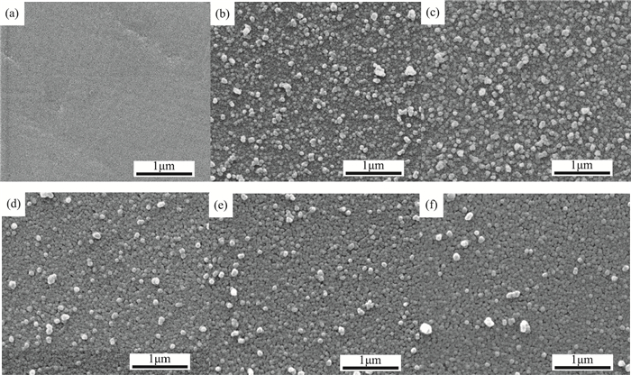

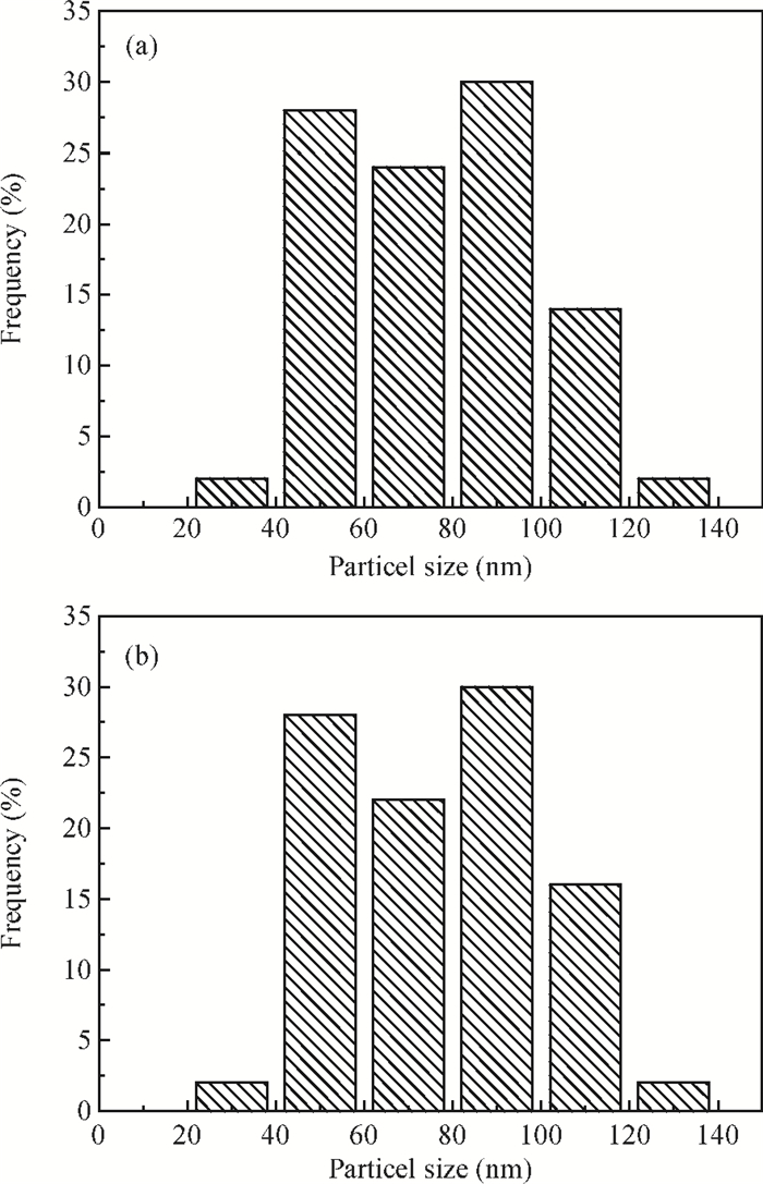
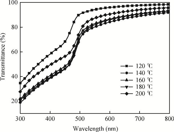
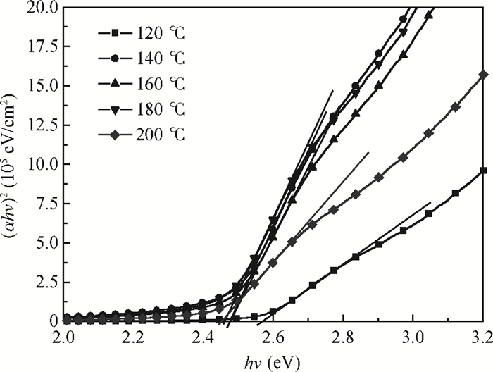
Table 1. Surface topology and values of average roughness (Ra) and root mean squared (RMS) roughness.

|
| [1] |
Li Wei, Feng Lianghuan, Cai Yaping, et al. Microstructure and properties of CdS polycrystalline thin films for solar cells. Chinese Journal of Semiconductors, 2005, 26(1):46 https://www.researchgate.net/publication/286013876_Microstructure_and_properties_of_CdS_polycrystalline_thin_films_for_solar_cells?ev=auth_pub
|
| [2] |
Senthil K, Mangalaraj D, Narayandass S K, et al. Argon and nitrogen implantation effects on the structural and optical properties of vacuum evaporated cadmium sulphide thin films. Semicond Sci Technol, 2002, 17(2):97 doi: 10.1088/0268-1242/17/2/302
|
| [3] |
Seo H K, Ok E A, Kim W M, et al. Electrical and optical characterization of the influence of chemical bath deposition time and temperature on CdS/Cu(In, Ga)Se2 junction properties in Cu(In, Ga)Se2 solar cells. Thin Solid Films, 2013, 546(1):289 http://www.sciencedirect.com/science/article/pii/S0040609013008390
|
| [4] |
Kosyachenko L A, Mathew X, Roshko V Y, et al. Optical absorptivity and recombination losses:The limitations imposed by the thickness of absorber layer in CdS/CdTe solar cells. Solar Energy Materials & Solar Cells, 2013, 114:179 http://www.sciencedirect.com/science/article/pii/S0927024813001165
|
| [5] |
Wang X, Yan X, Li W, et al. Doped quantum dots for white-light-emitting diodes without reabsorption of multiphase phosphors. Adv Mater, 2012, 24(20):2742 doi: 10.1002/adma.v24.20
|
| [6] |
Lin K, Tseng S, Chen H, et al. Ultrahigh-sensitivity CdS photoconductors with instant response and ultralow power consumption for detection in low-light environments. J Mater Chem C, 2013, 1(27):4244 doi: 10.1039/c3tc30520a
|
| [7] |
Lallan Y, Ritesh V, Dwivedi R. Sensing properties of CdS-doped tin oxide thick film gas sensor. Sensors and Actuators B, 2010, 144(1):37 doi: 10.1016/j.snb.2009.10.013
|
| [8] |
Raut B T, Godse P R, Pawar S G, et al. Novel method for fabrication of polyaniline-CdS sensor for H2S gas detection. Measurement, 2012, 45(1):94 doi: 10.1016/j.measurement.2011.09.015
|
| [9] |
Jia H, Hu Y, Tang Y, et al. Synthesis and photoelectrochemical behavior of nanocrystalline CdS film electrodes. Electrochemy Commun, 2006, 8(8):1381 doi: 10.1016/j.elecom.2006.06.025
|
| [10] |
Moualkia H, Hariech S, Aida M S. Structural and optical properties of CdS thin films grown by chemical bath deposition. Thin Solid Films, 2009, 518(4):1259 doi: 10.1016/j.tsf.2009.04.067
|
| [11] |
Liu F, Lai Y, Liu J, et al. Characterization of chemical bath deposited CdS thin films at different deposition temperature. Journal of Alloys and Compounds, 2010, 493(1):305 http://www.sciencedirect.com/science/article/pii/S0925838809026413
|
| [12] |
Ao Jianping, He Qing, Sun Guozhong, et al. Crystal structure and properties of chemical bath deposited CdS thin films. Chinese Journal of Semiconductors, 2005, 26(7):1347 http://en.cnki.com.cn/article_en/cjfdtotal-bdtx200507011.htm
|
| [13] |
Anil M P, Pranaya V J, Vedavati P, et al. Synthesis and X-ray single crystal structure of a cadmium(Ⅱ) acetophenone thiosemicarbazone complex and its use as a single-source precursor for the preparation of CdS nanocrystallites and thin films. Polyhedron, 2013, 61:195 doi: 10.1016/j.poly.2013.05.052
|
| [14] |
Kamila Z, Magdalena S. Electrodeposition of CdS from acidic aqueous thiosulfate solution-investigation of the mechanism by electrochemical quartz microbalance technique. Electrochimica Acta, 2011, 56(16):5731 doi: 10.1016/j.electacta.2011.04.046
|
| [15] |
Boieriu P, Sporken R, Adriaens A, et al. SIMS and XPS characterization of CdS/CdTe heterostructures grown by MBE. Nuclear Instruments and Methods in Physics Research B, 2000, 161-163:975 doi: 10.1016/S0168-583X(99)00926-X
|
| [16] |
Dhawale D S, Duba D P, Phadatare M R, et al. Synthesis and characterizations of CdS nanorods by SILAR method:effect of film thickness. J Mater Sci, 2011, 46(14):5009 doi: 10.1007/s10853-011-5421-z
|
| [17] |
Zhu G, Lv T, Pan L, et al. All spray pyrolysis deposited CdS sensitized ZnO films for quantum dot-sensitized solar cells. Journal of Alloys and Compounds, 2011, 509(2):362 doi: 10.1016/j.jallcom.2010.09.026
|
| [18] |
Feldmann C, Christof M. Polyol mediated synthesis of nanoscale MS particles (M = Zn, Cd, Hg). J Mater Chem, 2001, 11(10):2603 doi: 10.1039/b103167h
|
| [19] |
Quan Z, Li C, Zhang X, et al. Polyol-mediated synthesis of PbS crystals:Shape evolution and growth mechanism. Crystal Growth & Design, 2008, 8(7):2384 http://d.wanfangdata.com.cn/Periodical_NSTL_QKJJ028353061.aspx
|
| [20] |
Sorachon Y, Craig A G. Self-assembled TiO2 nanotube arrays by anodization of titanium in diethylene glycol:approach to extended pore pidening. Langmuir, 2010, 26(1):417 doi: 10.1021/la9020146
|
| [21] |
Feldmann C. Polyol-mediated synthesis of nanoscale functional materials. Adv Funct Mater, 2003, 13(2):101 doi: 10.1002/adfm.v13:2
|
| [22] |
Kurihara L K, Chow G M, Schoen P E. Nanocrystalline metallic powders and films produced by the polyol method. Nanostructured Materials, 1995, 5(6):607 doi: 10.1016/0965-9773(95)00275-J
|
| [23] |
Li Q, Bi D, Liu Z, et al. Characteristics and application of polyol method preparing ultrafine particles. Materials Science and Engineering of Powder Metallurgy, 2008, 13(2):79 http://en.cnki.com.cn/Article_en/CJFDTOTAL-FMGC200802002.htm
|
| [24] |
Senthil K, Mangalaraj D, Narayandass S K. Structural and optical properties of CdS thin flms. Appl Surf Sci, 2001, 169/170:476 doi: 10.1016/S0169-4332(00)00732-7
|
| [25] |
Chu J, Jin Z, Cai S, et al. An in-situ chemical reaction deposition of nanosized wurtzite CdS thin films. Thin Solid Films, 2012, 520(6):1826 doi: 10.1016/j.tsf.2011.08.101
|
| [26] |
Chen X, Zhang N, Sun K. Facile ammonia-induced fabrication of nanoporous NiO films with enhanced lithium-storage properties. Electrochem Commun, 2012, 20:137 doi: 10.1016/j.elecom.2012.04.009
|
| [27] |
Cortes A, Gomez H, Marotti R E, et al. Grain size dependence of the bandgap in chemical bathdeposited CdS thin films. Solar Energy Materials & Solar Cells, 2004, 82(1):21 http://www.sciencedirect.com/science/article/pii/S0927024804000030
|
| [28] |
Fan Ximei, Lian Jianshe, Guo Zuoxing, et al. Surface morphology and photoluminescence properties of ZnO thin films obtained by PLD. The Transactions of Nonferrous Metals Society of Chinese, 2005, 15(3):519 http://www.cqvip.com/Main/Detail.aspx?id=16033981
|
| [29] |
Li W, Cai X, Chen Q, et al. Influence of growth process on the structural, optical and electrical properties of CBD-CdS films. Mater Lett, 2005, 59(1):1 doi: 10.1016/j.matlet.2004.04.008
|
| [30] |
Metin H, Esen R. Annealing studies on CBD grown CdS thin films. J Cryst Growth, 2003, 258(1):141 http://www.sciencedirect.com/science/article/pii/S0022024803015185
|


Article views: 2703 Times PDF downloads: 9 Times Cited by: 0 Times
Received: 09 January 2014 Revised: 10 March 2014 Online: Published: 01 August 2014
| Citation: |
Fengzhang Zhang, Xiangqi Li, Xiaofeng Wu, Ximei Fan, Chaoliang Zhang. Influence of deposition temperature on CdS thin films by polyol method[J]. Journal of Semiconductors, 2014, 35(8): 083003. doi: 10.1088/1674-4926/35/8/083003
****
F Z Zhang, X Q Li, X F Wu, X M Fan, C L Zhang. Influence of deposition temperature on CdS thin films by polyol method[J]. J. Semicond., 2014, 35(8): 083003. doi: 10.1088/1674-4926/35/8/083003.

|
| [1] |
Li Wei, Feng Lianghuan, Cai Yaping, et al. Microstructure and properties of CdS polycrystalline thin films for solar cells. Chinese Journal of Semiconductors, 2005, 26(1):46 https://www.researchgate.net/publication/286013876_Microstructure_and_properties_of_CdS_polycrystalline_thin_films_for_solar_cells?ev=auth_pub
|
| [2] |
Senthil K, Mangalaraj D, Narayandass S K, et al. Argon and nitrogen implantation effects on the structural and optical properties of vacuum evaporated cadmium sulphide thin films. Semicond Sci Technol, 2002, 17(2):97 doi: 10.1088/0268-1242/17/2/302
|
| [3] |
Seo H K, Ok E A, Kim W M, et al. Electrical and optical characterization of the influence of chemical bath deposition time and temperature on CdS/Cu(In, Ga)Se2 junction properties in Cu(In, Ga)Se2 solar cells. Thin Solid Films, 2013, 546(1):289 http://www.sciencedirect.com/science/article/pii/S0040609013008390
|
| [4] |
Kosyachenko L A, Mathew X, Roshko V Y, et al. Optical absorptivity and recombination losses:The limitations imposed by the thickness of absorber layer in CdS/CdTe solar cells. Solar Energy Materials & Solar Cells, 2013, 114:179 http://www.sciencedirect.com/science/article/pii/S0927024813001165
|
| [5] |
Wang X, Yan X, Li W, et al. Doped quantum dots for white-light-emitting diodes without reabsorption of multiphase phosphors. Adv Mater, 2012, 24(20):2742 doi: 10.1002/adma.v24.20
|
| [6] |
Lin K, Tseng S, Chen H, et al. Ultrahigh-sensitivity CdS photoconductors with instant response and ultralow power consumption for detection in low-light environments. J Mater Chem C, 2013, 1(27):4244 doi: 10.1039/c3tc30520a
|
| [7] |
Lallan Y, Ritesh V, Dwivedi R. Sensing properties of CdS-doped tin oxide thick film gas sensor. Sensors and Actuators B, 2010, 144(1):37 doi: 10.1016/j.snb.2009.10.013
|
| [8] |
Raut B T, Godse P R, Pawar S G, et al. Novel method for fabrication of polyaniline-CdS sensor for H2S gas detection. Measurement, 2012, 45(1):94 doi: 10.1016/j.measurement.2011.09.015
|
| [9] |
Jia H, Hu Y, Tang Y, et al. Synthesis and photoelectrochemical behavior of nanocrystalline CdS film electrodes. Electrochemy Commun, 2006, 8(8):1381 doi: 10.1016/j.elecom.2006.06.025
|
| [10] |
Moualkia H, Hariech S, Aida M S. Structural and optical properties of CdS thin films grown by chemical bath deposition. Thin Solid Films, 2009, 518(4):1259 doi: 10.1016/j.tsf.2009.04.067
|
| [11] |
Liu F, Lai Y, Liu J, et al. Characterization of chemical bath deposited CdS thin films at different deposition temperature. Journal of Alloys and Compounds, 2010, 493(1):305 http://www.sciencedirect.com/science/article/pii/S0925838809026413
|
| [12] |
Ao Jianping, He Qing, Sun Guozhong, et al. Crystal structure and properties of chemical bath deposited CdS thin films. Chinese Journal of Semiconductors, 2005, 26(7):1347 http://en.cnki.com.cn/article_en/cjfdtotal-bdtx200507011.htm
|
| [13] |
Anil M P, Pranaya V J, Vedavati P, et al. Synthesis and X-ray single crystal structure of a cadmium(Ⅱ) acetophenone thiosemicarbazone complex and its use as a single-source precursor for the preparation of CdS nanocrystallites and thin films. Polyhedron, 2013, 61:195 doi: 10.1016/j.poly.2013.05.052
|
| [14] |
Kamila Z, Magdalena S. Electrodeposition of CdS from acidic aqueous thiosulfate solution-investigation of the mechanism by electrochemical quartz microbalance technique. Electrochimica Acta, 2011, 56(16):5731 doi: 10.1016/j.electacta.2011.04.046
|
| [15] |
Boieriu P, Sporken R, Adriaens A, et al. SIMS and XPS characterization of CdS/CdTe heterostructures grown by MBE. Nuclear Instruments and Methods in Physics Research B, 2000, 161-163:975 doi: 10.1016/S0168-583X(99)00926-X
|
| [16] |
Dhawale D S, Duba D P, Phadatare M R, et al. Synthesis and characterizations of CdS nanorods by SILAR method:effect of film thickness. J Mater Sci, 2011, 46(14):5009 doi: 10.1007/s10853-011-5421-z
|
| [17] |
Zhu G, Lv T, Pan L, et al. All spray pyrolysis deposited CdS sensitized ZnO films for quantum dot-sensitized solar cells. Journal of Alloys and Compounds, 2011, 509(2):362 doi: 10.1016/j.jallcom.2010.09.026
|
| [18] |
Feldmann C, Christof M. Polyol mediated synthesis of nanoscale MS particles (M = Zn, Cd, Hg). J Mater Chem, 2001, 11(10):2603 doi: 10.1039/b103167h
|
| [19] |
Quan Z, Li C, Zhang X, et al. Polyol-mediated synthesis of PbS crystals:Shape evolution and growth mechanism. Crystal Growth & Design, 2008, 8(7):2384 http://d.wanfangdata.com.cn/Periodical_NSTL_QKJJ028353061.aspx
|
| [20] |
Sorachon Y, Craig A G. Self-assembled TiO2 nanotube arrays by anodization of titanium in diethylene glycol:approach to extended pore pidening. Langmuir, 2010, 26(1):417 doi: 10.1021/la9020146
|
| [21] |
Feldmann C. Polyol-mediated synthesis of nanoscale functional materials. Adv Funct Mater, 2003, 13(2):101 doi: 10.1002/adfm.v13:2
|
| [22] |
Kurihara L K, Chow G M, Schoen P E. Nanocrystalline metallic powders and films produced by the polyol method. Nanostructured Materials, 1995, 5(6):607 doi: 10.1016/0965-9773(95)00275-J
|
| [23] |
Li Q, Bi D, Liu Z, et al. Characteristics and application of polyol method preparing ultrafine particles. Materials Science and Engineering of Powder Metallurgy, 2008, 13(2):79 http://en.cnki.com.cn/Article_en/CJFDTOTAL-FMGC200802002.htm
|
| [24] |
Senthil K, Mangalaraj D, Narayandass S K. Structural and optical properties of CdS thin flms. Appl Surf Sci, 2001, 169/170:476 doi: 10.1016/S0169-4332(00)00732-7
|
| [25] |
Chu J, Jin Z, Cai S, et al. An in-situ chemical reaction deposition of nanosized wurtzite CdS thin films. Thin Solid Films, 2012, 520(6):1826 doi: 10.1016/j.tsf.2011.08.101
|
| [26] |
Chen X, Zhang N, Sun K. Facile ammonia-induced fabrication of nanoporous NiO films with enhanced lithium-storage properties. Electrochem Commun, 2012, 20:137 doi: 10.1016/j.elecom.2012.04.009
|
| [27] |
Cortes A, Gomez H, Marotti R E, et al. Grain size dependence of the bandgap in chemical bathdeposited CdS thin films. Solar Energy Materials & Solar Cells, 2004, 82(1):21 http://www.sciencedirect.com/science/article/pii/S0927024804000030
|
| [28] |
Fan Ximei, Lian Jianshe, Guo Zuoxing, et al. Surface morphology and photoluminescence properties of ZnO thin films obtained by PLD. The Transactions of Nonferrous Metals Society of Chinese, 2005, 15(3):519 http://www.cqvip.com/Main/Detail.aspx?id=16033981
|
| [29] |
Li W, Cai X, Chen Q, et al. Influence of growth process on the structural, optical and electrical properties of CBD-CdS films. Mater Lett, 2005, 59(1):1 doi: 10.1016/j.matlet.2004.04.008
|
| [30] |
Metin H, Esen R. Annealing studies on CBD grown CdS thin films. J Cryst Growth, 2003, 258(1):141 http://www.sciencedirect.com/science/article/pii/S0022024803015185
|

 WeChat ID
Journal of Semiconductors © 2017 All Rights Reserved 京ICP备05085259号-2

 DownLoad: