


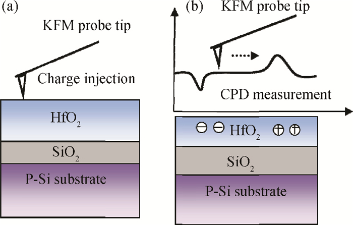
Fig. 1.
Schematic sample structure and KFM analysis method (a) charge injection with contact mode and (b) contact potential differences (CPDs) measurement.
SEMICONDUCTOR MATERIALS
Yuqiong Chu, Zongliang Huo, Yulong Han, Guoxing Chen, Dong Zhang, Xinkai Li and Ming Liu
Corresponding author: Huo Zongliang, Email:huozongliang@ime.ac.cn; Liu Ming, Email:liuming@ime.ac.cn
Abstract: The retention characteristics of electrons and holes in hafnium oxide with post-deposition annealing in a N2 or O2 ambient were investigated by Kelvin probe force microscopy. The KFM results show that compared with the N2 PDA process, the O2 PDA process can lead to a significant retention improvement. Vertical charge leakage and lateral charge spreading both played an important role in the charge loss mechanisms. The retention improvement is attributed to the deeper trap energy. For electrons, the trap energy of the HOS structure annealed in a N2 or O2 ambient were determined to be about 0.44 and 0.49 eV, respectively. For holes, these are about 0.34 and 0.36 eV, respectively. Finally, the electrical characteristics of the memory devices are demonstrated from the experiment, which agreed with our characterization results. The qualitative and quantitative determination of the charge retention properties, the possible charge decay mechanism and trap energy reported in this work can be very useful for the characterization of hafnium charge storage devices.
| [1] |
Kim K. From the future Si technology perspective:challenges and opportunities. Electron Devices Meeting, 2010, 1(1):1 http://ieeexplore.ieee.org/xpls/icp.jsp?arnumber=5703274
|
| [2] |
Wang Y Q, Hwang W S, Zhang G, et al. Electrical characteristics of memory devices with a high-k HfO2 trapping layer and dual SiO2/Si3N4 tunneling layer. IEEE Trans Electron Devices, 2007, 54(10):2700 http://ieeexplore.ieee.org/document/4317755/
|
| [3] |
You H W, Cho W J. Charge trapping properties of the HfO2 layer with various thicknesses for charge trap flash memory applications. Appl Phys Lett, 2010, 96(9):093506 doi: 10.1063/1.3337103
|
| [4] |
Yuan C L, Chan M Y, Lee P S, et al. Al2O3 nanocrystals embedded in amorphous Lu2O3 high-k gate dielectric for floating gate memory application. J Phys:Conference Series, 2007, 61(1):1312 http://adsabs.harvard.edu/abs/2007JPhCS..61.1312Y
|
| [5] |
Ding S J, Zhang D W, Wang L K. Atomic-layer-deposited Al2O3-HfO2 laminated and sandwiched dielectrics for metal-insulator-metal capacitors. J Phys D:Appl Phys, 2007, 40(4):1072 doi: 10.1088/0022-3727/40/4/023
|
| [6] |
Maikap S, Rahaman S Z, Tien T C, et al. Nanoscale (EOT = 5.6 nm) nonvolatile memory characteristics using n-Si/SiO2/HfAlO nanocrystal/Al2O3/Pt capacitors. Nanotechnology, 2008, 19(43):435202 doi: 10.1088/0957-4484/19/43/435202
|
| [7] |
Sugizaki T, Kohayashi M, Ishidao M, et al. Novel multi-bit SONOS type flash memory using a high-k charge trapping layer. Symposium on VLSI Technology, 2003:27 http://ieeexplore.ieee.org/xpls/icp.jsp?arnumber=1221069
|
| [8] |
Spiga S, Driussi F, Lamperti A. Experimental and simulation study of the program efficiency of HfO2 based charge trapping memories. Solid-State Device Research Conference (ESSDERC), 2010:408 http://ieeexplore.ieee.org/abstract/document/5618194/
|
| [9] |
Zhu Chenxin, Yang Rong, Huo Zongliang, et al. Investigation of charge trap and loss characteristics for charge trap memory by electrostatic force microscopy. Non-Volatile Memory Technology Symposium (NVMTS), 2011:1 http://ieeexplore.ieee.org/document/6137099/
|
| [10] |
Chowdhury N A, Garg R, Misra D, et al. Charge trapping and interface characteristics of thermally evaporated HfO2. Appl Phys Lett, 2004, 85(15):3290 doi: 10.1063/1.1805708
|
| [11] |
Ryan J T, Yu L C, Han J H, et al. A new interface defect spectroscopy method. IRPS, 2011:203 http://ieeexplore.ieee.org/document/5872242/
|
| [12] |
Uren M J. The properties of individual Si/SiO2 defects and their link to 1/f noise. Mater Sci Forum, 1992, 83-87:1519 doi: 10.4028/www.scientific.net/MSF.83-87
|
| [13] |
Girard P. Electrostatic force microscopy:principles and some applications to semiconductors. Nanotechnology, 2001, 12(4):485 doi: 10.1088/0957-4484/12/4/321
|
| [14] |
Tzeng S D, Gwo S. Charge trapping properties at silicon nitride/silicon oxide interface studied by variable-temperature electrostatic force microscopy. J Appl Phys, 2006, 100(2):023711 doi: 10.1063/1.2218025
|
| [15] |
Baik S J, Lim K S. Lateral redistribution of trapped charges in nitride/oxide/Si (NOS) investigated by electrostatic force microscopy. Nanoscale, 2011, 3:2560 doi: 10.1039/c1nr10104h
|
| [16] |
Chen Yong, Zhao Jianming, Han Dedong, et al. Extraction of equivalent oxide thickness for HfO2 high k gate dielectrics. Chinese Journal of Semiconductors, 2006, 27(5):852
|
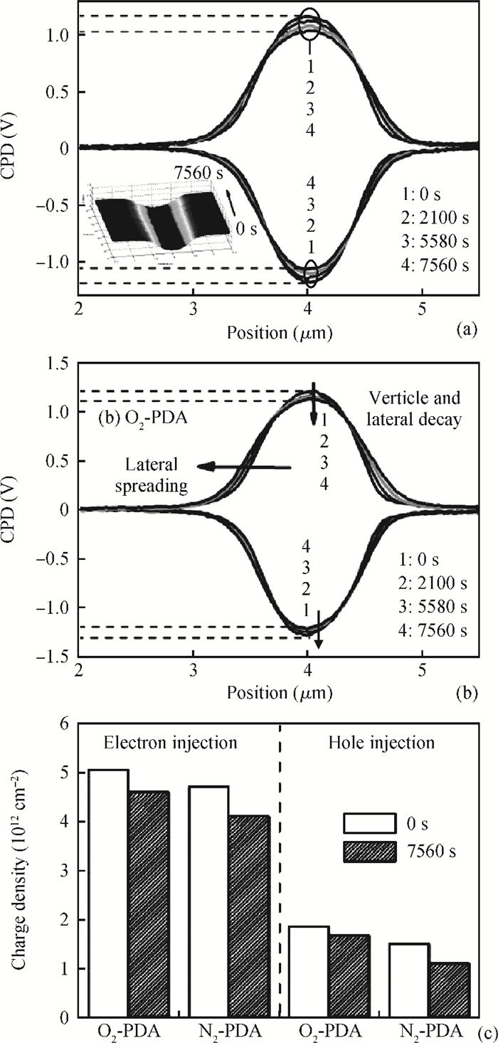

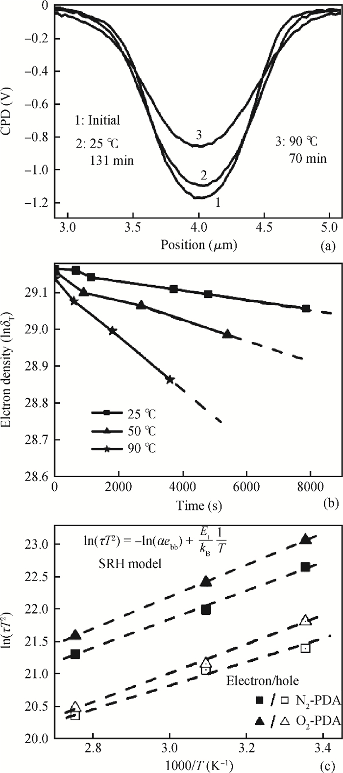
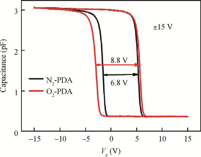
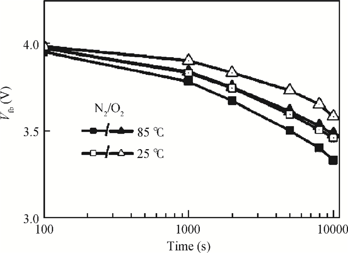

Table 1. Extracted diffusion coefficients for different samples.

|
Table 2. Extracted trap energy levels for different samples. Unit: eV

|
| [1] |
Kim K. From the future Si technology perspective:challenges and opportunities. Electron Devices Meeting, 2010, 1(1):1 http://ieeexplore.ieee.org/xpls/icp.jsp?arnumber=5703274
|
| [2] |
Wang Y Q, Hwang W S, Zhang G, et al. Electrical characteristics of memory devices with a high-k HfO2 trapping layer and dual SiO2/Si3N4 tunneling layer. IEEE Trans Electron Devices, 2007, 54(10):2700 http://ieeexplore.ieee.org/document/4317755/
|
| [3] |
You H W, Cho W J. Charge trapping properties of the HfO2 layer with various thicknesses for charge trap flash memory applications. Appl Phys Lett, 2010, 96(9):093506 doi: 10.1063/1.3337103
|
| [4] |
Yuan C L, Chan M Y, Lee P S, et al. Al2O3 nanocrystals embedded in amorphous Lu2O3 high-k gate dielectric for floating gate memory application. J Phys:Conference Series, 2007, 61(1):1312 http://adsabs.harvard.edu/abs/2007JPhCS..61.1312Y
|
| [5] |
Ding S J, Zhang D W, Wang L K. Atomic-layer-deposited Al2O3-HfO2 laminated and sandwiched dielectrics for metal-insulator-metal capacitors. J Phys D:Appl Phys, 2007, 40(4):1072 doi: 10.1088/0022-3727/40/4/023
|
| [6] |
Maikap S, Rahaman S Z, Tien T C, et al. Nanoscale (EOT = 5.6 nm) nonvolatile memory characteristics using n-Si/SiO2/HfAlO nanocrystal/Al2O3/Pt capacitors. Nanotechnology, 2008, 19(43):435202 doi: 10.1088/0957-4484/19/43/435202
|
| [7] |
Sugizaki T, Kohayashi M, Ishidao M, et al. Novel multi-bit SONOS type flash memory using a high-k charge trapping layer. Symposium on VLSI Technology, 2003:27 http://ieeexplore.ieee.org/xpls/icp.jsp?arnumber=1221069
|
| [8] |
Spiga S, Driussi F, Lamperti A. Experimental and simulation study of the program efficiency of HfO2 based charge trapping memories. Solid-State Device Research Conference (ESSDERC), 2010:408 http://ieeexplore.ieee.org/abstract/document/5618194/
|
| [9] |
Zhu Chenxin, Yang Rong, Huo Zongliang, et al. Investigation of charge trap and loss characteristics for charge trap memory by electrostatic force microscopy. Non-Volatile Memory Technology Symposium (NVMTS), 2011:1 http://ieeexplore.ieee.org/document/6137099/
|
| [10] |
Chowdhury N A, Garg R, Misra D, et al. Charge trapping and interface characteristics of thermally evaporated HfO2. Appl Phys Lett, 2004, 85(15):3290 doi: 10.1063/1.1805708
|
| [11] |
Ryan J T, Yu L C, Han J H, et al. A new interface defect spectroscopy method. IRPS, 2011:203 http://ieeexplore.ieee.org/document/5872242/
|
| [12] |
Uren M J. The properties of individual Si/SiO2 defects and their link to 1/f noise. Mater Sci Forum, 1992, 83-87:1519 doi: 10.4028/www.scientific.net/MSF.83-87
|
| [13] |
Girard P. Electrostatic force microscopy:principles and some applications to semiconductors. Nanotechnology, 2001, 12(4):485 doi: 10.1088/0957-4484/12/4/321
|
| [14] |
Tzeng S D, Gwo S. Charge trapping properties at silicon nitride/silicon oxide interface studied by variable-temperature electrostatic force microscopy. J Appl Phys, 2006, 100(2):023711 doi: 10.1063/1.2218025
|
| [15] |
Baik S J, Lim K S. Lateral redistribution of trapped charges in nitride/oxide/Si (NOS) investigated by electrostatic force microscopy. Nanoscale, 2011, 3:2560 doi: 10.1039/c1nr10104h
|
| [16] |
Chen Yong, Zhao Jianming, Han Dedong, et al. Extraction of equivalent oxide thickness for HfO2 high k gate dielectrics. Chinese Journal of Semiconductors, 2006, 27(5):852
|


Article views: 2850 Times PDF downloads: 34 Times Cited by: 0 Times
Received: 10 January 2014 Revised: 10 March 2014 Online: Published: 01 August 2014
| Citation: |
Yuqiong Chu, Zongliang Huo, Yulong Han, Guoxing Chen, Dong Zhang, Xinkai Li, Ming Liu. Investigation of charge loss characteristics of HfO2 annealed in N2 or O2 ambient[J]. Journal of Semiconductors, 2014, 35(8): 083004. doi: 10.1088/1674-4926/35/8/083004
****
Y Q Chu, Z L Huo, Y L Han, G X Chen, D Zhang, X K Li, M Liu. Investigation of charge loss characteristics of HfO2 annealed in N2 or O2 ambient[J]. J. Semicond., 2014, 35(8): 083004. doi: 10.1088/1674-4926/35/8/083004.

|
| [1] |
Kim K. From the future Si technology perspective:challenges and opportunities. Electron Devices Meeting, 2010, 1(1):1 http://ieeexplore.ieee.org/xpls/icp.jsp?arnumber=5703274
|
| [2] |
Wang Y Q, Hwang W S, Zhang G, et al. Electrical characteristics of memory devices with a high-k HfO2 trapping layer and dual SiO2/Si3N4 tunneling layer. IEEE Trans Electron Devices, 2007, 54(10):2700 http://ieeexplore.ieee.org/document/4317755/
|
| [3] |
You H W, Cho W J. Charge trapping properties of the HfO2 layer with various thicknesses for charge trap flash memory applications. Appl Phys Lett, 2010, 96(9):093506 doi: 10.1063/1.3337103
|
| [4] |
Yuan C L, Chan M Y, Lee P S, et al. Al2O3 nanocrystals embedded in amorphous Lu2O3 high-k gate dielectric for floating gate memory application. J Phys:Conference Series, 2007, 61(1):1312 http://adsabs.harvard.edu/abs/2007JPhCS..61.1312Y
|
| [5] |
Ding S J, Zhang D W, Wang L K. Atomic-layer-deposited Al2O3-HfO2 laminated and sandwiched dielectrics for metal-insulator-metal capacitors. J Phys D:Appl Phys, 2007, 40(4):1072 doi: 10.1088/0022-3727/40/4/023
|
| [6] |
Maikap S, Rahaman S Z, Tien T C, et al. Nanoscale (EOT = 5.6 nm) nonvolatile memory characteristics using n-Si/SiO2/HfAlO nanocrystal/Al2O3/Pt capacitors. Nanotechnology, 2008, 19(43):435202 doi: 10.1088/0957-4484/19/43/435202
|
| [7] |
Sugizaki T, Kohayashi M, Ishidao M, et al. Novel multi-bit SONOS type flash memory using a high-k charge trapping layer. Symposium on VLSI Technology, 2003:27 http://ieeexplore.ieee.org/xpls/icp.jsp?arnumber=1221069
|
| [8] |
Spiga S, Driussi F, Lamperti A. Experimental and simulation study of the program efficiency of HfO2 based charge trapping memories. Solid-State Device Research Conference (ESSDERC), 2010:408 http://ieeexplore.ieee.org/abstract/document/5618194/
|
| [9] |
Zhu Chenxin, Yang Rong, Huo Zongliang, et al. Investigation of charge trap and loss characteristics for charge trap memory by electrostatic force microscopy. Non-Volatile Memory Technology Symposium (NVMTS), 2011:1 http://ieeexplore.ieee.org/document/6137099/
|
| [10] |
Chowdhury N A, Garg R, Misra D, et al. Charge trapping and interface characteristics of thermally evaporated HfO2. Appl Phys Lett, 2004, 85(15):3290 doi: 10.1063/1.1805708
|
| [11] |
Ryan J T, Yu L C, Han J H, et al. A new interface defect spectroscopy method. IRPS, 2011:203 http://ieeexplore.ieee.org/document/5872242/
|
| [12] |
Uren M J. The properties of individual Si/SiO2 defects and their link to 1/f noise. Mater Sci Forum, 1992, 83-87:1519 doi: 10.4028/www.scientific.net/MSF.83-87
|
| [13] |
Girard P. Electrostatic force microscopy:principles and some applications to semiconductors. Nanotechnology, 2001, 12(4):485 doi: 10.1088/0957-4484/12/4/321
|
| [14] |
Tzeng S D, Gwo S. Charge trapping properties at silicon nitride/silicon oxide interface studied by variable-temperature electrostatic force microscopy. J Appl Phys, 2006, 100(2):023711 doi: 10.1063/1.2218025
|
| [15] |
Baik S J, Lim K S. Lateral redistribution of trapped charges in nitride/oxide/Si (NOS) investigated by electrostatic force microscopy. Nanoscale, 2011, 3:2560 doi: 10.1039/c1nr10104h
|
| [16] |
Chen Yong, Zhao Jianming, Han Dedong, et al. Extraction of equivalent oxide thickness for HfO2 high k gate dielectrics. Chinese Journal of Semiconductors, 2006, 27(5):852
|

 WeChat ID
Journal of Semiconductors © 2017 All Rights Reserved 京ICP备05085259号-2

 DownLoad:

