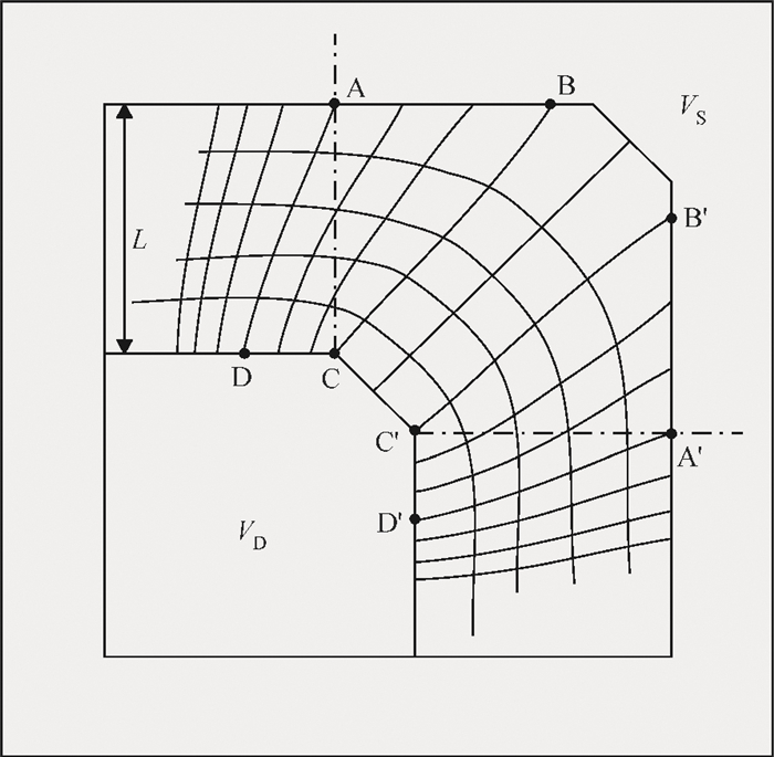
Fig. 1.
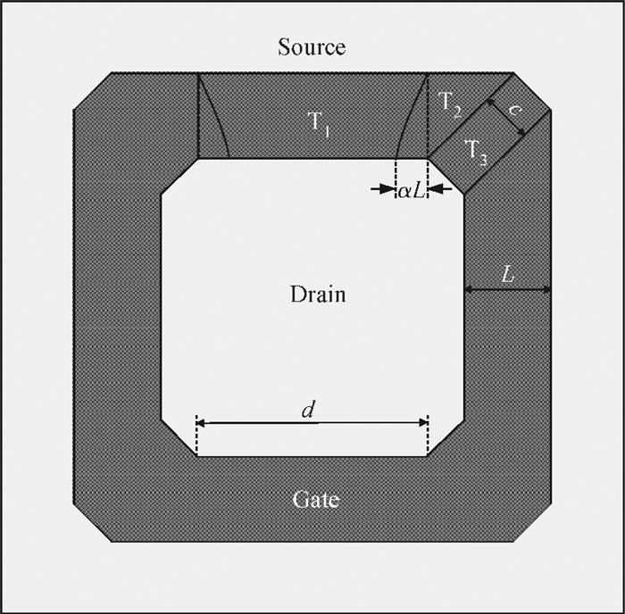
Layout diagram of the ELT
SEMICONDUCTOR INTEGRATED CIRCUITS
Jia Zhang1, 2, Haigang Yang1, , Jiabin Sun1, Le Yu1 and Yuanfeng Wei1
Corresponding author: Yang Haigang, Email:yanghg@mail.ie.ac.cn
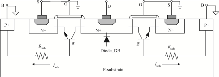
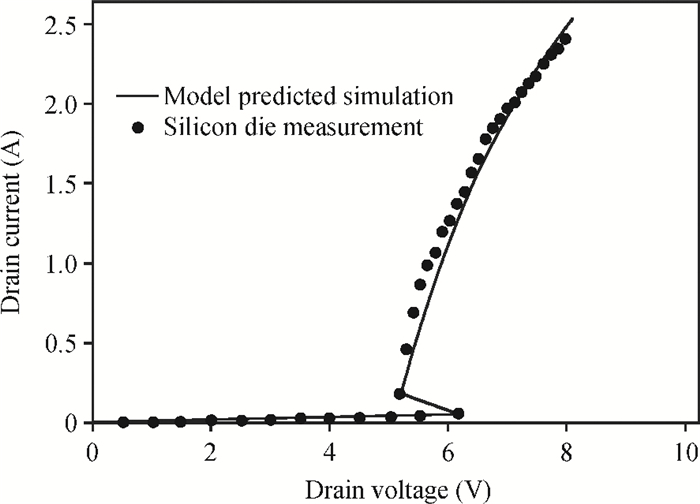
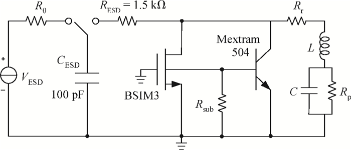
Abstract: This paper proposes a novel technique for modeling the electrostatic discharge (ESD) characteristic of the enclosed-gate layout transistors (ELTs). The model consists of an ELT, a parasitic bipolar transistor, and a substrate resistor. The ELT is decomposed into edge and corner transistors by solving the electrostatic field problem through the conformal mapping method, and these transistors are separately modeled by BSIM (Berkeley Short-channel IGFET Model). Fast simulation speed and easy implementation is obtained as the model can be incorporated into standard SPICE simulation. The model parameters are extracted from the critical point of the snapback curve, and simulation results are presented and compared to experimental data for verification.
Keywords: Electrostatic discharge, Enclosed-gate layout transistor, modeling, conformal mapping
| [1] |
Lee M S, Lee H C. Dummy gate-assisted n-MOSFET layout for a radiation-tolerant integrated circuit. IEEE Trans Nucl Sci, 2013, 60(4):3084 doi: 10.1109/TNS.2013.2268390
|
| [2] |
Nowlin R, McEndree S, Wilson A, et al. A new total-dose-induced parasitic effect in enclosed-geometry transistors. IEEE Trans Nucl Sci, 2005, 52(6):2495 doi: 10.1109/TNS.2005.860713
|
| [3] |
VSilvestri M, Gerardin S, Paccagnella A, et al. Degradation induced by X-ray irradiation and channel hot carrier stresses in 130-nm NMOSFETs with enclosed layout. IEEE Trans Nucl Sci, 2008, 55(6):3216 doi: 10.1109/TNS.2008.2006747
|
| [4] |
Ker M D, Wu C Y, Wu T S. Area-efficient layout design for CMOS output transistors. IEEE Trans Electron Devices, 1997, 44(4):635 doi: 10.1109/16.563369
|
| [5] |
Champion C L, Rue G S L. Accurate SPICE models for CMOS analog radiation-hardness-by-design. IEEE Trans Nucl Sci, 2005, 52(6):2542 doi: 10.1109/TNS.2005.860717
|
| [6] |
Chen L, Gingrich D M. Study of n-channel MOSFETs with an enclosed-gate layout in a 0.18μm CMOS technology. IEEE Trans Nucl Sci, 2005, 52(4):861 doi: 10.1109/TNS.2005.852652
|
| [7] |
Jiao C, Yu Z. A robust novel technique for SPICE simulation of ESD snapback characteristic. Proceedings of the 8th International Conference on Solid-State Integrated Circuit Technology, 2006:1367 http://ieeexplore.ieee.org/xpl/articleDetails.jsp?arnumber=4098411&openedRefinements%3D*%26filter%3DAND%28AND%28NOT%284283010803%29%29%2CAND%28NOT%284283010803%29%29%29%26pageNumber%3D7%26rowsPerPage%3D100%26queryText%3D%28esd%29
|
| [8] |
Vassilev V, Lorenzini M, Groeseneken G. MOSFET ESD breakdown modeling and parameter extraction in advanced CMOS technologies. IEEE Trans Electron Devices, 2006, 53(9):2108 doi: 10.1109/TED.2006.880367
|
| [9] |
Li J, Joshi S, Rosenbaum E. A verilog-a compact model for ESD protection NMOSTs. Proceedings of Custom Integrated Circuits Conference, 2003:253
|
| [10] |
Gao X, Liou J, Bernier J, et al. Implementation of a comprehensive and robust MOSFET model in cadence SPICE for ESD applications. IEEE Trans Computer-Aided Design of Integrated Circuits and Systems, 2002, 21(12):1497 doi: 10.1109/TCAD.2002.804379
|
| [11] |
Zhou Y Z, Connerney D, Carroll R, et al. Modeling MOS snapback for circuit-level ESD simulation using BSIM3 and VBIC models. Proceedings of the 6th International Symposium on Quality Electronic Design, San Jose, 2005:476 doi: 10.1109/ISQED.2005.81
|
| [12] |
Giraldo A, Paccagnella A, Minzoni A. Aspect ratio calculation in n-channel MOSFETs with a gate-enclosed layout. Solid-State Electron, 2000, 44:981 doi: 10.1016/S0038-1101(00)00010-1
|
| [13] |
Liu W D, Jin X D, Chen J, et al. BSIM3v3. 2. 2 MOSFET model users' manual. Department of Electrical Engineering and Computer Sciences University of California, Berkeley, 1999
|
| [14] |
Van der Toorn R, Paasschens J C J, Kloosterman W J. The Mextram bipolar transistor model, level 504. 10. 1. Users' Manual, Koninklijke Philips Electronics N. V. , Amsterdam, Netherlands, 2000/2004
|
| [15] |
Chen S H, Ker M D, Hung H P. Active ESD protection design for interface circuits between separated power domains against cross-power-domain ESD stresses. IEEE Trans Device Mater Reliab, 2008, 8(3):549 doi: 10.1109/TDMR.2008.2002492
|
| [16] |
Meng K H, Rosenbaum E. Verification of snapback model by transient I-V measurement for circuit simulation of ESD response. IEEE Trans Device Mater Reliab, 2013, 13(2):371 doi: 10.1109/TDMR.2013.2258672
|
| [17] |
Amerasekera A, Ramaswamy S, Chang M, et al. Modeling MOS snapback and parasitic bipolar action for circuit-level ESD and high current simulations. Proceedings of the 34th Annual IEEE International Reliability Physics Symposium, Dallas, 1996:318
|
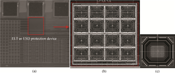
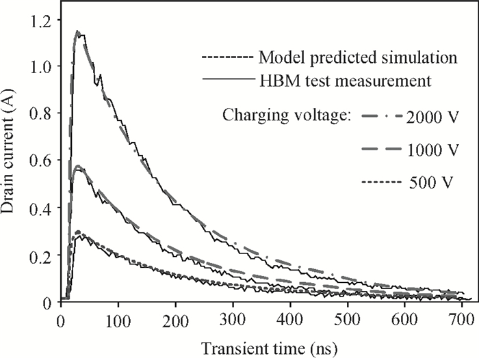
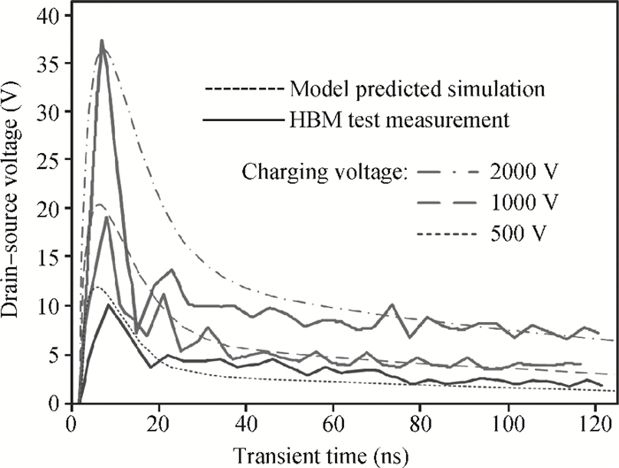
Table 1.
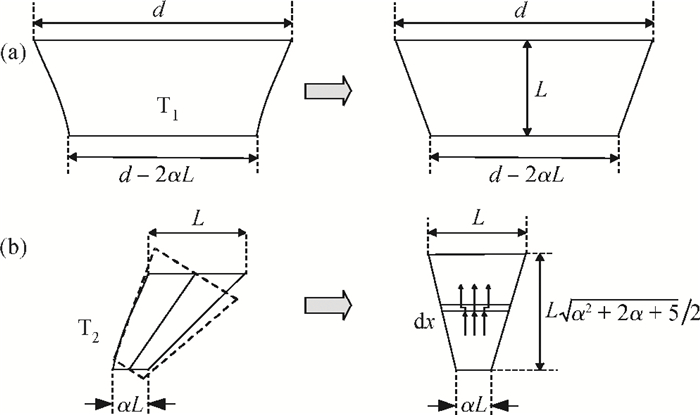
The effective channel width and length of T

|
Table 2. Critical parameters of the snapback curve

|
Table 3. Parameters extracted from measurements

|
| [1] |
Lee M S, Lee H C. Dummy gate-assisted n-MOSFET layout for a radiation-tolerant integrated circuit. IEEE Trans Nucl Sci, 2013, 60(4):3084 doi: 10.1109/TNS.2013.2268390
|
| [2] |
Nowlin R, McEndree S, Wilson A, et al. A new total-dose-induced parasitic effect in enclosed-geometry transistors. IEEE Trans Nucl Sci, 2005, 52(6):2495 doi: 10.1109/TNS.2005.860713
|
| [3] |
VSilvestri M, Gerardin S, Paccagnella A, et al. Degradation induced by X-ray irradiation and channel hot carrier stresses in 130-nm NMOSFETs with enclosed layout. IEEE Trans Nucl Sci, 2008, 55(6):3216 doi: 10.1109/TNS.2008.2006747
|
| [4] |
Ker M D, Wu C Y, Wu T S. Area-efficient layout design for CMOS output transistors. IEEE Trans Electron Devices, 1997, 44(4):635 doi: 10.1109/16.563369
|
| [5] |
Champion C L, Rue G S L. Accurate SPICE models for CMOS analog radiation-hardness-by-design. IEEE Trans Nucl Sci, 2005, 52(6):2542 doi: 10.1109/TNS.2005.860717
|
| [6] |
Chen L, Gingrich D M. Study of n-channel MOSFETs with an enclosed-gate layout in a 0.18μm CMOS technology. IEEE Trans Nucl Sci, 2005, 52(4):861 doi: 10.1109/TNS.2005.852652
|
| [7] |
Jiao C, Yu Z. A robust novel technique for SPICE simulation of ESD snapback characteristic. Proceedings of the 8th International Conference on Solid-State Integrated Circuit Technology, 2006:1367 http://ieeexplore.ieee.org/xpl/articleDetails.jsp?arnumber=4098411&openedRefinements%3D*%26filter%3DAND%28AND%28NOT%284283010803%29%29%2CAND%28NOT%284283010803%29%29%29%26pageNumber%3D7%26rowsPerPage%3D100%26queryText%3D%28esd%29
|
| [8] |
Vassilev V, Lorenzini M, Groeseneken G. MOSFET ESD breakdown modeling and parameter extraction in advanced CMOS technologies. IEEE Trans Electron Devices, 2006, 53(9):2108 doi: 10.1109/TED.2006.880367
|
| [9] |
Li J, Joshi S, Rosenbaum E. A verilog-a compact model for ESD protection NMOSTs. Proceedings of Custom Integrated Circuits Conference, 2003:253
|
| [10] |
Gao X, Liou J, Bernier J, et al. Implementation of a comprehensive and robust MOSFET model in cadence SPICE for ESD applications. IEEE Trans Computer-Aided Design of Integrated Circuits and Systems, 2002, 21(12):1497 doi: 10.1109/TCAD.2002.804379
|
| [11] |
Zhou Y Z, Connerney D, Carroll R, et al. Modeling MOS snapback for circuit-level ESD simulation using BSIM3 and VBIC models. Proceedings of the 6th International Symposium on Quality Electronic Design, San Jose, 2005:476 doi: 10.1109/ISQED.2005.81
|
| [12] |
Giraldo A, Paccagnella A, Minzoni A. Aspect ratio calculation in n-channel MOSFETs with a gate-enclosed layout. Solid-State Electron, 2000, 44:981 doi: 10.1016/S0038-1101(00)00010-1
|
| [13] |
Liu W D, Jin X D, Chen J, et al. BSIM3v3. 2. 2 MOSFET model users' manual. Department of Electrical Engineering and Computer Sciences University of California, Berkeley, 1999
|
| [14] |
Van der Toorn R, Paasschens J C J, Kloosterman W J. The Mextram bipolar transistor model, level 504. 10. 1. Users' Manual, Koninklijke Philips Electronics N. V. , Amsterdam, Netherlands, 2000/2004
|
| [15] |
Chen S H, Ker M D, Hung H P. Active ESD protection design for interface circuits between separated power domains against cross-power-domain ESD stresses. IEEE Trans Device Mater Reliab, 2008, 8(3):549 doi: 10.1109/TDMR.2008.2002492
|
| [16] |
Meng K H, Rosenbaum E. Verification of snapback model by transient I-V measurement for circuit simulation of ESD response. IEEE Trans Device Mater Reliab, 2013, 13(2):371 doi: 10.1109/TDMR.2013.2258672
|
| [17] |
Amerasekera A, Ramaswamy S, Chang M, et al. Modeling MOS snapback and parasitic bipolar action for circuit-level ESD and high current simulations. Proceedings of the 34th Annual IEEE International Reliability Physics Symposium, Dallas, 1996:318
|


Article views: 5132 Times PDF downloads: 44 Times Cited by: 0 Times
Received: 14 January 2014 Revised: 27 January 2014 Online: Published: 01 August 2014
| Citation: |
Jia Zhang, Haigang Yang, Jiabin Sun, Le Yu, Yuanfeng Wei. Modeling of enclosed-gate layout transistors as ESD protection device based on conformal mapping method[J]. Journal of Semiconductors, 2014, 35(8): 085001. doi: 10.1088/1674-4926/35/8/085001
****
J Zhang, H G Yang, J B Sun, L Yu, Y F Wei. Modeling of enclosed-gate layout transistors as ESD protection device based on conformal mapping method[J]. J. Semicond., 2014, 35(8): 085001. doi: 10.1088/1674-4926/35/8/085001.

|
| [1] |
Lee M S, Lee H C. Dummy gate-assisted n-MOSFET layout for a radiation-tolerant integrated circuit. IEEE Trans Nucl Sci, 2013, 60(4):3084 doi: 10.1109/TNS.2013.2268390
|
| [2] |
Nowlin R, McEndree S, Wilson A, et al. A new total-dose-induced parasitic effect in enclosed-geometry transistors. IEEE Trans Nucl Sci, 2005, 52(6):2495 doi: 10.1109/TNS.2005.860713
|
| [3] |
VSilvestri M, Gerardin S, Paccagnella A, et al. Degradation induced by X-ray irradiation and channel hot carrier stresses in 130-nm NMOSFETs with enclosed layout. IEEE Trans Nucl Sci, 2008, 55(6):3216 doi: 10.1109/TNS.2008.2006747
|
| [4] |
Ker M D, Wu C Y, Wu T S. Area-efficient layout design for CMOS output transistors. IEEE Trans Electron Devices, 1997, 44(4):635 doi: 10.1109/16.563369
|
| [5] |
Champion C L, Rue G S L. Accurate SPICE models for CMOS analog radiation-hardness-by-design. IEEE Trans Nucl Sci, 2005, 52(6):2542 doi: 10.1109/TNS.2005.860717
|
| [6] |
Chen L, Gingrich D M. Study of n-channel MOSFETs with an enclosed-gate layout in a 0.18μm CMOS technology. IEEE Trans Nucl Sci, 2005, 52(4):861 doi: 10.1109/TNS.2005.852652
|
| [7] |
Jiao C, Yu Z. A robust novel technique for SPICE simulation of ESD snapback characteristic. Proceedings of the 8th International Conference on Solid-State Integrated Circuit Technology, 2006:1367 http://ieeexplore.ieee.org/xpl/articleDetails.jsp?arnumber=4098411&openedRefinements%3D*%26filter%3DAND%28AND%28NOT%284283010803%29%29%2CAND%28NOT%284283010803%29%29%29%26pageNumber%3D7%26rowsPerPage%3D100%26queryText%3D%28esd%29
|
| [8] |
Vassilev V, Lorenzini M, Groeseneken G. MOSFET ESD breakdown modeling and parameter extraction in advanced CMOS technologies. IEEE Trans Electron Devices, 2006, 53(9):2108 doi: 10.1109/TED.2006.880367
|
| [9] |
Li J, Joshi S, Rosenbaum E. A verilog-a compact model for ESD protection NMOSTs. Proceedings of Custom Integrated Circuits Conference, 2003:253
|
| [10] |
Gao X, Liou J, Bernier J, et al. Implementation of a comprehensive and robust MOSFET model in cadence SPICE for ESD applications. IEEE Trans Computer-Aided Design of Integrated Circuits and Systems, 2002, 21(12):1497 doi: 10.1109/TCAD.2002.804379
|
| [11] |
Zhou Y Z, Connerney D, Carroll R, et al. Modeling MOS snapback for circuit-level ESD simulation using BSIM3 and VBIC models. Proceedings of the 6th International Symposium on Quality Electronic Design, San Jose, 2005:476 doi: 10.1109/ISQED.2005.81
|
| [12] |
Giraldo A, Paccagnella A, Minzoni A. Aspect ratio calculation in n-channel MOSFETs with a gate-enclosed layout. Solid-State Electron, 2000, 44:981 doi: 10.1016/S0038-1101(00)00010-1
|
| [13] |
Liu W D, Jin X D, Chen J, et al. BSIM3v3. 2. 2 MOSFET model users' manual. Department of Electrical Engineering and Computer Sciences University of California, Berkeley, 1999
|
| [14] |
Van der Toorn R, Paasschens J C J, Kloosterman W J. The Mextram bipolar transistor model, level 504. 10. 1. Users' Manual, Koninklijke Philips Electronics N. V. , Amsterdam, Netherlands, 2000/2004
|
| [15] |
Chen S H, Ker M D, Hung H P. Active ESD protection design for interface circuits between separated power domains against cross-power-domain ESD stresses. IEEE Trans Device Mater Reliab, 2008, 8(3):549 doi: 10.1109/TDMR.2008.2002492
|
| [16] |
Meng K H, Rosenbaum E. Verification of snapback model by transient I-V measurement for circuit simulation of ESD response. IEEE Trans Device Mater Reliab, 2013, 13(2):371 doi: 10.1109/TDMR.2013.2258672
|
| [17] |
Amerasekera A, Ramaswamy S, Chang M, et al. Modeling MOS snapback and parasitic bipolar action for circuit-level ESD and high current simulations. Proceedings of the 34th Annual IEEE International Reliability Physics Symposium, Dallas, 1996:318
|

 WeChat ID
Journal of Semiconductors © 2017 All Rights Reserved 京ICP备05085259号-2

 DownLoad: