


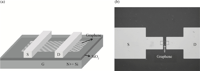
Fig. 1.
(a) Structure schematic diagram and (b) optical microscope graph of graphene field effect transistor, ${W}{\text{/}}{L}{\text{ = 10 }}\mu {\text{m/10 }}\mu {\text{m}}$ .
SEMICONDUCTOR DEVICES
Jie Yang1, , Kunpeng Jia1, Yajuan Su1, , Yang Chen2 and Chao Zhao1
Corresponding author: Jie Yang, yangjie11@mails.ucas.ac.cn; Su Yajuan, Email:suyajuan@ime.ac.cn
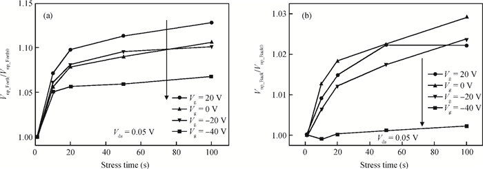
Abstract: The current transport characteristic is studied systematically based on a back-gate graphene field effect transistor, under repeated test and gate voltage stress. The interface trapped charges caused by the gate voltage sweep process screens the gate electric field, and results in the neutral point voltage shift between the forth and back sweep direction. In the repeated test process, the neutral point voltage keeps increasing with test times in both forth and back sweeps, which indicates the existence of interface trapped electrons residual and accumulation. In gate voltage stress experiment, the relative neutral point voltage significantly decreases with the reducing of stress voltage, especially in -40 V, which illustrates the driven-out phenomenon of trapped electrons under negative voltage stress.
Keywords: graphene FET, interface trap, electrical measurement, repeated test, stress
| [1] |
Novoselov K S, Geim A K, Morozov S V, et al. Electric field effect in atomically thin carbon films. Science, 2004, 306:666 doi: 10.1126/science.1102896
|
| [2] |
Bolotin K I, Sikes K J, Jiang Z, et al. Ultrahigh electron mobility in suspended graphene. Solid-State Commun, 2008, 146:351 doi: 10.1016/j.ssc.2008.02.024
|
| [3] |
Nair R R, Blake P, Grigorenko A N, et al. Fine structure constant defines visual transparency of graphene. Science, 2008, 320:1308 doi: 10.1126/science.1156965
|
| [4] |
Bonaccorso F, Sun Z, Hasan T, et al. Graphene photonics and optoelectronics. Nat Photonics, 2010, 4:611 doi: 10.1038/nphoton.2010.186
|
| [5] |
Wu Y Q, Farmer D B, Valdes-Garcia A, et al. Record high RF performance for epitaxial graphene transistors. IEEE International Electron Devices Meeting (IEDM), 2011 http://ieeexplore.ieee.org/document/6131601/
|
| [6] |
Wang X, Zhi L J, Mullen K. Transparent, conductive graphene electrodes for dye-sensitized solar cells. Nano Lett, 2008, 8:323 doi: 10.1021/nl072838r
|
| [7] |
Hicks J, Tejeda A, Taleb-Ibrahimi A, et al. A wide-bandgap metal-semiconductor-metal nanostructure made entirely from graphene. Nat Phys, 2013, 9:49 http://www.nature.com/nphys/journal/v9/n1/full/nphys2487.html?foxtrotcallback=true
|
| [8] |
Chiu H Y, Perebeinos V, Lin Y M, et al. Controllable p-n junction formation in mono layer graphene using electrostatic substrate engineering. Nano Lett, 2010, 10:4634 doi: 10.1021/nl102756r
|
| [9] |
Yang Y X, Brenner K, Murali R. The influence of atmosphere on electrical transport in graphene. Carbon, 2012, 50:1727 doi: 10.1016/j.carbon.2011.12.008
|
| [10] |
Wang H M, Wu Y H, Cong C X, et al. Hysteresis of electronic transport in graphene transistors. Acs Nano, 2010, 4:7221 doi: 10.1021/nn101950n
|
| [11] |
Lafkioti M, Krauss B, Lohmann T, et al. Graphene on a hydrophobic substrate:doping reduction and hysteresis suppression under ambient conditions. Nano Lett, 2010, 10:1149 doi: 10.1021/nl903162a
|
| [12] |
Kim W, Javey A, Vermesh O, et al. Hysteresis caused by water molecules in carbon nanotube field-effect transistors. Nano Lett, 2003, 3:193 doi: 10.1021/nl0259232
|
| [13] |
Jia Kunpeng, Yang Jie, Su Yajuan, et al. Stability analysis of a back-gate graphene transistor in air environment. Journal of Semiconductors, 2013, 34:084004 doi: 10.1088/1674-4926/34/8/084004
|
| [14] |
Yang Y X, Murali R. Binding mechanisms of molecular oxygen and moisture to graphene. Appl Phys Lett, 2011, 98(9):093116 doi: 10.1063/1.3562317
|
| [15] |
Ferrari A C, Meyer J C, Scardaci V, et al. Raman spectrum of graphene and graphene layers. Phys Rev Lett, 2006, 97:187401 doi: 10.1103/PhysRevLett.97.187401
|
| [16] |
Das A, Pisana S, Chakraborty B, et al. Monitoring dopants by Raman scattering in an electrochemically top-gated graphene transistor. Nature Nanotechnology, 2008, 3:210 doi: 10.1038/nnano.2008.67
|
| [17] |
Moser J, Barreiro A, Bachtold A. Current-induced cleaning of graphene. Appl Phys Lett, 2007, 91:163513 doi: 10.1063/1.2789673
|
| [18] |
Liao Z M, Han B H, Zhou Y B, et al. Hysteresis reversion in graphene field-effect transistors. J Chem Phys, 2010, 133:044703 doi: 10.1063/1.3460798
|


Article views: 4516 Times PDF downloads: 76 Times Cited by: 0 Times
Received: 24 January 2014 Revised: 21 March 2014 Online: Published: 01 September 2014
| Citation: |
Jie Yang, Kunpeng Jia, Yajuan Su, Yang Chen, Chao Zhao. Hysteresis analysis of graphene transistor under repeated test and gate voltage stress[J]. Journal of Semiconductors, 2014, 35(9): 094003. doi: 10.1088/1674-4926/35/9/094003
****
J Yang, K P Jia, Y J Su, Y Chen, C Zhao. Hysteresis analysis of graphene transistor under repeated test and gate voltage stress[J]. J. Semicond., 2014, 35(9): 094003. doi: 10.1088/1674-4926/35/9/094003.

|
| [1] |
Novoselov K S, Geim A K, Morozov S V, et al. Electric field effect in atomically thin carbon films. Science, 2004, 306:666 doi: 10.1126/science.1102896
|
| [2] |
Bolotin K I, Sikes K J, Jiang Z, et al. Ultrahigh electron mobility in suspended graphene. Solid-State Commun, 2008, 146:351 doi: 10.1016/j.ssc.2008.02.024
|
| [3] |
Nair R R, Blake P, Grigorenko A N, et al. Fine structure constant defines visual transparency of graphene. Science, 2008, 320:1308 doi: 10.1126/science.1156965
|
| [4] |
Bonaccorso F, Sun Z, Hasan T, et al. Graphene photonics and optoelectronics. Nat Photonics, 2010, 4:611 doi: 10.1038/nphoton.2010.186
|
| [5] |
Wu Y Q, Farmer D B, Valdes-Garcia A, et al. Record high RF performance for epitaxial graphene transistors. IEEE International Electron Devices Meeting (IEDM), 2011 http://ieeexplore.ieee.org/document/6131601/
|
| [6] |
Wang X, Zhi L J, Mullen K. Transparent, conductive graphene electrodes for dye-sensitized solar cells. Nano Lett, 2008, 8:323 doi: 10.1021/nl072838r
|
| [7] |
Hicks J, Tejeda A, Taleb-Ibrahimi A, et al. A wide-bandgap metal-semiconductor-metal nanostructure made entirely from graphene. Nat Phys, 2013, 9:49 http://www.nature.com/nphys/journal/v9/n1/full/nphys2487.html?foxtrotcallback=true
|
| [8] |
Chiu H Y, Perebeinos V, Lin Y M, et al. Controllable p-n junction formation in mono layer graphene using electrostatic substrate engineering. Nano Lett, 2010, 10:4634 doi: 10.1021/nl102756r
|
| [9] |
Yang Y X, Brenner K, Murali R. The influence of atmosphere on electrical transport in graphene. Carbon, 2012, 50:1727 doi: 10.1016/j.carbon.2011.12.008
|
| [10] |
Wang H M, Wu Y H, Cong C X, et al. Hysteresis of electronic transport in graphene transistors. Acs Nano, 2010, 4:7221 doi: 10.1021/nn101950n
|
| [11] |
Lafkioti M, Krauss B, Lohmann T, et al. Graphene on a hydrophobic substrate:doping reduction and hysteresis suppression under ambient conditions. Nano Lett, 2010, 10:1149 doi: 10.1021/nl903162a
|
| [12] |
Kim W, Javey A, Vermesh O, et al. Hysteresis caused by water molecules in carbon nanotube field-effect transistors. Nano Lett, 2003, 3:193 doi: 10.1021/nl0259232
|
| [13] |
Jia Kunpeng, Yang Jie, Su Yajuan, et al. Stability analysis of a back-gate graphene transistor in air environment. Journal of Semiconductors, 2013, 34:084004 doi: 10.1088/1674-4926/34/8/084004
|
| [14] |
Yang Y X, Murali R. Binding mechanisms of molecular oxygen and moisture to graphene. Appl Phys Lett, 2011, 98(9):093116 doi: 10.1063/1.3562317
|
| [15] |
Ferrari A C, Meyer J C, Scardaci V, et al. Raman spectrum of graphene and graphene layers. Phys Rev Lett, 2006, 97:187401 doi: 10.1103/PhysRevLett.97.187401
|
| [16] |
Das A, Pisana S, Chakraborty B, et al. Monitoring dopants by Raman scattering in an electrochemically top-gated graphene transistor. Nature Nanotechnology, 2008, 3:210 doi: 10.1038/nnano.2008.67
|
| [17] |
Moser J, Barreiro A, Bachtold A. Current-induced cleaning of graphene. Appl Phys Lett, 2007, 91:163513 doi: 10.1063/1.2789673
|
| [18] |
Liao Z M, Han B H, Zhou Y B, et al. Hysteresis reversion in graphene field-effect transistors. J Chem Phys, 2010, 133:044703 doi: 10.1063/1.3460798
|

 WeChat ID
Journal of Semiconductors © 2017 All Rights Reserved 京ICP备05085259号-2

 DownLoad:

