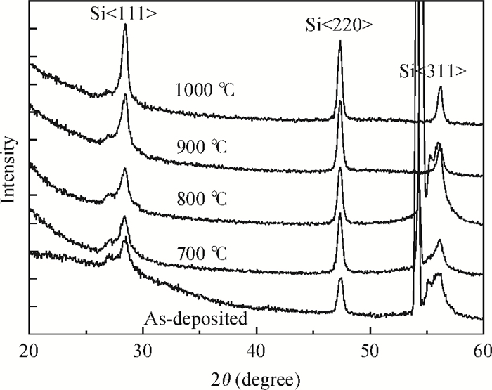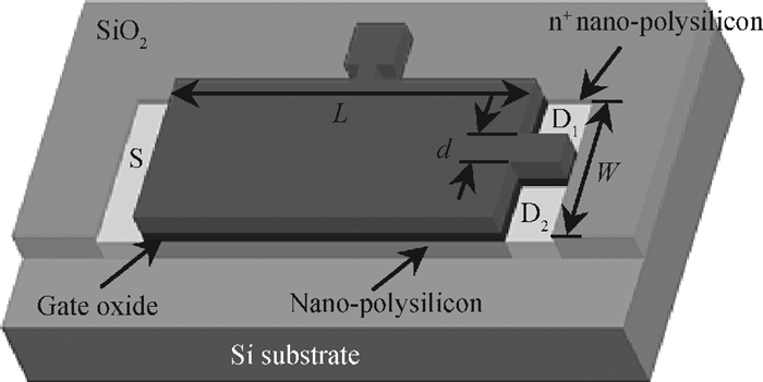
Fig. 1.
Basic structure of the split-drain MAGFET based on nanopolysilicon TFT.
SEMICONDUCTOR DEVICES
Xiaofeng Zhao, Dianzhong Wen, Meiwei Lü, Hanyu Guan and Gang Liu
Corresponding author: Wen Dianzhong, Email:wendianzhong@hlju.edu.cn
Abstract: A split-drain magnetic field-effect transistor (MAGFET) based on a nano-polysilicon thin film transistor (TFT) is proposed, which contains one source, two drains and one gate. The sensor chips were fabricated on < 100angle high resistivity silicon substrate by CMOS technology. When drain-source voltage equals 5.0 V and length and width ratio of the TFT channel is 80 μm/160 μm, the current and voltage magnetic sensitivities of the split-drain MAGFET based on the TFT are 0.018 mA/T and 55 mV/T, respectively. Through adopting nano-polysilicon thin films and nano-polysilicon thin films/high resistivity silicon heterojunction interfaces as the magnetic sensing layers, it is possible to realize detection of the external magnetic field. The test results show that magnetic sensitivity of the split-drain MAGFET can be improved significantly.
Keywords: nano-polysilicon thin films, thin film transistor, split-drain MAGFET, CMOS technology, heterojunction interfaces
| [1] |
Gallagher R C, Corak W S. A metal-oxide-semiconductor (MOS) Hall element. Solid-State Electron, 1966, 9:571 doi: 10.1016/0038-1101(66)90172-9
|
| [2] |
Sung G M. Error correction for transformed concave and convex MAGFETs with DC supply voltage. Sensors and Actuators A:Physical, 2005, 117(1):41 doi: 10.1016/j.sna.2004.04.053
|
| [3] |
Yao Yunruo, Zhu Dazhong. Sector split-drain MAGFET structure and model based on standard CMOS technology. Chinese Journal of Semiconductors, 2005, 26(4):751(in Chinese) http://ieeexplore.ieee.org/document/1435162/authors
|
| [4] |
Yao Y, Zhu D, Guo Q. Sector split-drain magnetic field-effect transistor based on standard CMOS technology. Sensors and Actuators A:Physical, 2005, 121(2):347 doi: 10.1016/j.sna.2005.02.029
|
| [5] |
Guo Q, Zhu D, Yao Y. CMOS magnetic sensor integrated circuit with sectorial MAGFET. Sensors and Actuators A:Physical, 2006, 126(1):154 doi: 10.1016/j.sna.2005.10.004
|
| [6] |
Liu Tong, Zhu Dazhong. Relative sensitivity of sector split-drain magnetic field-effect transistor based on geometrical correction factor of sector Hall plate. Chinese Journal of Semiconductors, 2006, 27(12):2155(in Chinese) http://ieeexplore.ieee.org/document/4098379/
|
| [7] |
Chen S L, Kuo C H, Liu S I. CMOS magnetic field to frequency converter. IEEE Sensors Journal, 2003, 3(2):241 doi: 10.1109/JSEN.2002.807485
|
| [8] |
Santillan-Quiñonez G F, Champac V, Murphy R S. Exploiting magnetic sensing capabilities of short split-drain MAGFETs. Solid-State Electron, 2010, 54:1239 doi: 10.1016/j.sse.2010.06.016
|
| [9] |
Hasan S M R. A novel 0.7 V high sensitivity complementary differential MAGFET sensor for contactless mechatronic applications. Sensors and Actuators A:Physical, 2010, 163(1):138 doi: 10.1016/j.sna.2010.08.009
|
| [10] |
Zhao Xiaofeng, Wen Dianzhong. Fabrication and characteristics of the nc-Si/c-Si heterojunction MAGFET. Journal of Semiconductors, 2009, 30(11):114002 doi: 10.1088/1674-4926/30/11/114002
|
| [11] |
Wei W, Wang T, He Y, et al. Investigation on high mobility nanocrystalline Si with crystalline Si heterostructure. Superlattices and Microstructures, 2007, 41(4):216 doi: 10.1016/j.spmi.2006.12.002
|
| [12] |
Wei Wensheng. Detection of carrier information in heterojunctions of nanocrystalline/crystalline Si. Solid State Sci, 2010, (12):789 http://www.sciencedirect.com/science/article/pii/S1293255810000828
|
| [13] |
Chen X Y, Sheng W Z, He Y L. Enhancement of electron mobility in nanocrystalline silicon/crystalline silicon heterostructures. J App Phys, 2005, (97):024305 doi: 10.1063/1.1832752
|
| [14] |
Chuai Rongyan, Wang Jian, Wu Meile, et al. A tunneling piezoresistive model for polysilicon. Journal of Semiconductors, 2012, 33(9):092003 doi: 10.1088/1674-4926/33/9/092003
|
| [15] |
Bihan F L, Carvou E, Fortin B, et al. Realization of polycrystalline silicon magnetic sensors. Sensors and Actuators A:Physical, 2001, 88(2):133 doi: 10.1016/S0924-4247(00)00506-9
|
| [16] |
Carvou E, Bihan F L, Bonnaud O. Hall effect magnetic sensors based on polysilicon TFTs. IEEE Sensors Journal, 2004, 4(5):597 doi: 10.1109/JSEN.2004.833497
|
| [17] |
Yamaguchi Y, Hashimoto H, Kimura M, et al. Magnetic-field area sensor using poly-Si micro Hall devices. IEEE Electron Device Lett, 2010, 31(11):1260 doi: 10.1109/LED.2010.2068271
|
| [18] |
Kimura M, Yamaguchi Y, Hashimoto H, et al. Analysis of Hall voltage in micro poly-Si Hall cells. Electrochem Solid-State Lett, 2010, 13(8):J96 doi: 10.1149/1.3436663
|
| [19] |
Zhao Xiaofeng, Wen Dianzhong, Zhuang Cuicui, et al. Fabrication and characteristics of the magnetic field sensors based on nano-polysilicon thin-film transistors. Journal of Semiconductors, 2013, 34(3):036001 doi: 10.1088/1674-4926/34/3/036001
|
| [20] |
Zhao Xiaofeng, Wen Dianzhong, Zhuang Cuicui, et al. High sensitivity magnetic field sensors based on nano-polysilicon thin-film transistors. Chinese Physics Letters, 2012, 29(11):118501 doi: 10.1088/0256-307X/29/11/118501
|
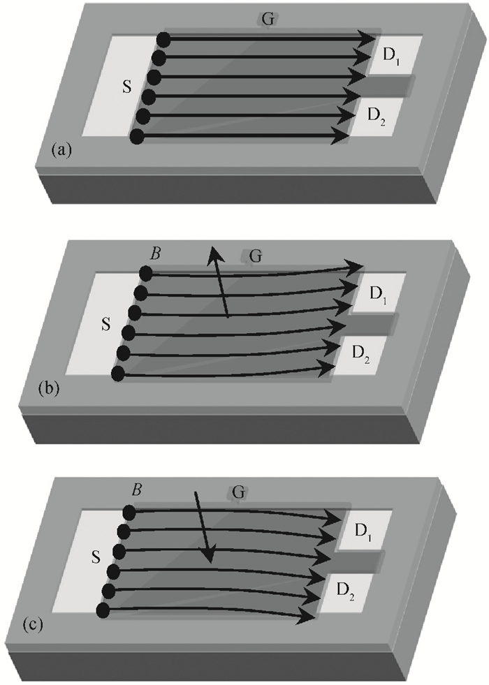
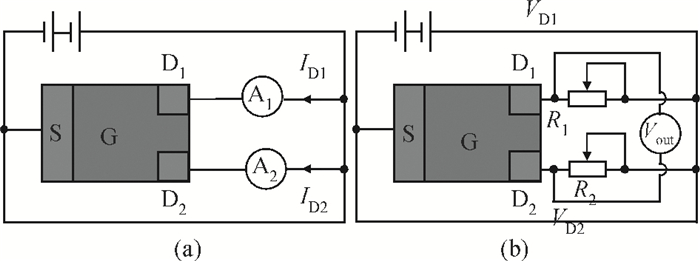
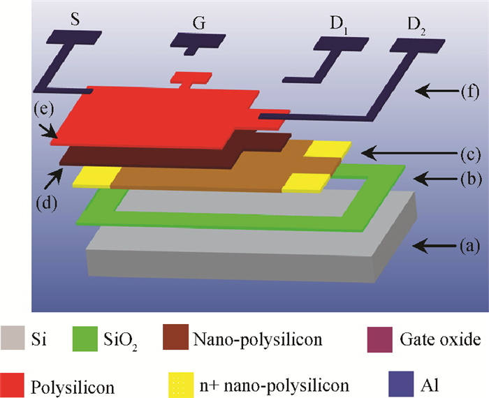
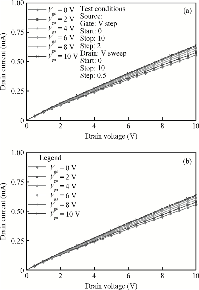
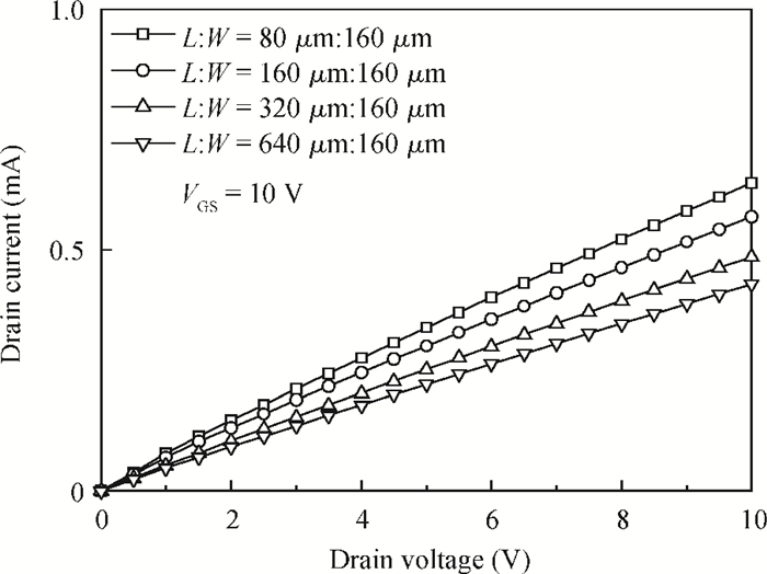
Table 1. Magnetic sensitivities of current and voltage of the split-drain MAGFET based on the nano-polysilicon TFT

|
| [1] |
Gallagher R C, Corak W S. A metal-oxide-semiconductor (MOS) Hall element. Solid-State Electron, 1966, 9:571 doi: 10.1016/0038-1101(66)90172-9
|
| [2] |
Sung G M. Error correction for transformed concave and convex MAGFETs with DC supply voltage. Sensors and Actuators A:Physical, 2005, 117(1):41 doi: 10.1016/j.sna.2004.04.053
|
| [3] |
Yao Yunruo, Zhu Dazhong. Sector split-drain MAGFET structure and model based on standard CMOS technology. Chinese Journal of Semiconductors, 2005, 26(4):751(in Chinese) http://ieeexplore.ieee.org/document/1435162/authors
|
| [4] |
Yao Y, Zhu D, Guo Q. Sector split-drain magnetic field-effect transistor based on standard CMOS technology. Sensors and Actuators A:Physical, 2005, 121(2):347 doi: 10.1016/j.sna.2005.02.029
|
| [5] |
Guo Q, Zhu D, Yao Y. CMOS magnetic sensor integrated circuit with sectorial MAGFET. Sensors and Actuators A:Physical, 2006, 126(1):154 doi: 10.1016/j.sna.2005.10.004
|
| [6] |
Liu Tong, Zhu Dazhong. Relative sensitivity of sector split-drain magnetic field-effect transistor based on geometrical correction factor of sector Hall plate. Chinese Journal of Semiconductors, 2006, 27(12):2155(in Chinese) http://ieeexplore.ieee.org/document/4098379/
|
| [7] |
Chen S L, Kuo C H, Liu S I. CMOS magnetic field to frequency converter. IEEE Sensors Journal, 2003, 3(2):241 doi: 10.1109/JSEN.2002.807485
|
| [8] |
Santillan-Quiñonez G F, Champac V, Murphy R S. Exploiting magnetic sensing capabilities of short split-drain MAGFETs. Solid-State Electron, 2010, 54:1239 doi: 10.1016/j.sse.2010.06.016
|
| [9] |
Hasan S M R. A novel 0.7 V high sensitivity complementary differential MAGFET sensor for contactless mechatronic applications. Sensors and Actuators A:Physical, 2010, 163(1):138 doi: 10.1016/j.sna.2010.08.009
|
| [10] |
Zhao Xiaofeng, Wen Dianzhong. Fabrication and characteristics of the nc-Si/c-Si heterojunction MAGFET. Journal of Semiconductors, 2009, 30(11):114002 doi: 10.1088/1674-4926/30/11/114002
|
| [11] |
Wei W, Wang T, He Y, et al. Investigation on high mobility nanocrystalline Si with crystalline Si heterostructure. Superlattices and Microstructures, 2007, 41(4):216 doi: 10.1016/j.spmi.2006.12.002
|
| [12] |
Wei Wensheng. Detection of carrier information in heterojunctions of nanocrystalline/crystalline Si. Solid State Sci, 2010, (12):789 http://www.sciencedirect.com/science/article/pii/S1293255810000828
|
| [13] |
Chen X Y, Sheng W Z, He Y L. Enhancement of electron mobility in nanocrystalline silicon/crystalline silicon heterostructures. J App Phys, 2005, (97):024305 doi: 10.1063/1.1832752
|
| [14] |
Chuai Rongyan, Wang Jian, Wu Meile, et al. A tunneling piezoresistive model for polysilicon. Journal of Semiconductors, 2012, 33(9):092003 doi: 10.1088/1674-4926/33/9/092003
|
| [15] |
Bihan F L, Carvou E, Fortin B, et al. Realization of polycrystalline silicon magnetic sensors. Sensors and Actuators A:Physical, 2001, 88(2):133 doi: 10.1016/S0924-4247(00)00506-9
|
| [16] |
Carvou E, Bihan F L, Bonnaud O. Hall effect magnetic sensors based on polysilicon TFTs. IEEE Sensors Journal, 2004, 4(5):597 doi: 10.1109/JSEN.2004.833497
|
| [17] |
Yamaguchi Y, Hashimoto H, Kimura M, et al. Magnetic-field area sensor using poly-Si micro Hall devices. IEEE Electron Device Lett, 2010, 31(11):1260 doi: 10.1109/LED.2010.2068271
|
| [18] |
Kimura M, Yamaguchi Y, Hashimoto H, et al. Analysis of Hall voltage in micro poly-Si Hall cells. Electrochem Solid-State Lett, 2010, 13(8):J96 doi: 10.1149/1.3436663
|
| [19] |
Zhao Xiaofeng, Wen Dianzhong, Zhuang Cuicui, et al. Fabrication and characteristics of the magnetic field sensors based on nano-polysilicon thin-film transistors. Journal of Semiconductors, 2013, 34(3):036001 doi: 10.1088/1674-4926/34/3/036001
|
| [20] |
Zhao Xiaofeng, Wen Dianzhong, Zhuang Cuicui, et al. High sensitivity magnetic field sensors based on nano-polysilicon thin-film transistors. Chinese Physics Letters, 2012, 29(11):118501 doi: 10.1088/0256-307X/29/11/118501
|


Article views: 3585 Times PDF downloads: 29 Times Cited by: 0 Times
Received: 04 February 2014 Revised: 13 March 2014 Online: Published: 01 September 2014
| Citation: |
Xiaofeng Zhao, Dianzhong Wen, Meiwei Lü, Hanyu Guan, Gang Liu. Fabrication and characterization of the split-drain MAGFET based on the nano-polysilicon thin film transistor[J]. Journal of Semiconductors, 2014, 35(9): 094004. doi: 10.1088/1674-4926/35/9/094004
****
X F Zhao, D Z Wen, M Lü, H Y Guan, G Liu. Fabrication and characterization of the split-drain MAGFET based on the nano-polysilicon thin film transistor[J]. J. Semicond., 2014, 35(9): 094004. doi: 10.1088/1674-4926/35/9/094004.

|
| [1] |
Gallagher R C, Corak W S. A metal-oxide-semiconductor (MOS) Hall element. Solid-State Electron, 1966, 9:571 doi: 10.1016/0038-1101(66)90172-9
|
| [2] |
Sung G M. Error correction for transformed concave and convex MAGFETs with DC supply voltage. Sensors and Actuators A:Physical, 2005, 117(1):41 doi: 10.1016/j.sna.2004.04.053
|
| [3] |
Yao Yunruo, Zhu Dazhong. Sector split-drain MAGFET structure and model based on standard CMOS technology. Chinese Journal of Semiconductors, 2005, 26(4):751(in Chinese) http://ieeexplore.ieee.org/document/1435162/authors
|
| [4] |
Yao Y, Zhu D, Guo Q. Sector split-drain magnetic field-effect transistor based on standard CMOS technology. Sensors and Actuators A:Physical, 2005, 121(2):347 doi: 10.1016/j.sna.2005.02.029
|
| [5] |
Guo Q, Zhu D, Yao Y. CMOS magnetic sensor integrated circuit with sectorial MAGFET. Sensors and Actuators A:Physical, 2006, 126(1):154 doi: 10.1016/j.sna.2005.10.004
|
| [6] |
Liu Tong, Zhu Dazhong. Relative sensitivity of sector split-drain magnetic field-effect transistor based on geometrical correction factor of sector Hall plate. Chinese Journal of Semiconductors, 2006, 27(12):2155(in Chinese) http://ieeexplore.ieee.org/document/4098379/
|
| [7] |
Chen S L, Kuo C H, Liu S I. CMOS magnetic field to frequency converter. IEEE Sensors Journal, 2003, 3(2):241 doi: 10.1109/JSEN.2002.807485
|
| [8] |
Santillan-Quiñonez G F, Champac V, Murphy R S. Exploiting magnetic sensing capabilities of short split-drain MAGFETs. Solid-State Electron, 2010, 54:1239 doi: 10.1016/j.sse.2010.06.016
|
| [9] |
Hasan S M R. A novel 0.7 V high sensitivity complementary differential MAGFET sensor for contactless mechatronic applications. Sensors and Actuators A:Physical, 2010, 163(1):138 doi: 10.1016/j.sna.2010.08.009
|
| [10] |
Zhao Xiaofeng, Wen Dianzhong. Fabrication and characteristics of the nc-Si/c-Si heterojunction MAGFET. Journal of Semiconductors, 2009, 30(11):114002 doi: 10.1088/1674-4926/30/11/114002
|
| [11] |
Wei W, Wang T, He Y, et al. Investigation on high mobility nanocrystalline Si with crystalline Si heterostructure. Superlattices and Microstructures, 2007, 41(4):216 doi: 10.1016/j.spmi.2006.12.002
|
| [12] |
Wei Wensheng. Detection of carrier information in heterojunctions of nanocrystalline/crystalline Si. Solid State Sci, 2010, (12):789 http://www.sciencedirect.com/science/article/pii/S1293255810000828
|
| [13] |
Chen X Y, Sheng W Z, He Y L. Enhancement of electron mobility in nanocrystalline silicon/crystalline silicon heterostructures. J App Phys, 2005, (97):024305 doi: 10.1063/1.1832752
|
| [14] |
Chuai Rongyan, Wang Jian, Wu Meile, et al. A tunneling piezoresistive model for polysilicon. Journal of Semiconductors, 2012, 33(9):092003 doi: 10.1088/1674-4926/33/9/092003
|
| [15] |
Bihan F L, Carvou E, Fortin B, et al. Realization of polycrystalline silicon magnetic sensors. Sensors and Actuators A:Physical, 2001, 88(2):133 doi: 10.1016/S0924-4247(00)00506-9
|
| [16] |
Carvou E, Bihan F L, Bonnaud O. Hall effect magnetic sensors based on polysilicon TFTs. IEEE Sensors Journal, 2004, 4(5):597 doi: 10.1109/JSEN.2004.833497
|
| [17] |
Yamaguchi Y, Hashimoto H, Kimura M, et al. Magnetic-field area sensor using poly-Si micro Hall devices. IEEE Electron Device Lett, 2010, 31(11):1260 doi: 10.1109/LED.2010.2068271
|
| [18] |
Kimura M, Yamaguchi Y, Hashimoto H, et al. Analysis of Hall voltage in micro poly-Si Hall cells. Electrochem Solid-State Lett, 2010, 13(8):J96 doi: 10.1149/1.3436663
|
| [19] |
Zhao Xiaofeng, Wen Dianzhong, Zhuang Cuicui, et al. Fabrication and characteristics of the magnetic field sensors based on nano-polysilicon thin-film transistors. Journal of Semiconductors, 2013, 34(3):036001 doi: 10.1088/1674-4926/34/3/036001
|
| [20] |
Zhao Xiaofeng, Wen Dianzhong, Zhuang Cuicui, et al. High sensitivity magnetic field sensors based on nano-polysilicon thin-film transistors. Chinese Physics Letters, 2012, 29(11):118501 doi: 10.1088/0256-307X/29/11/118501
|

 WeChat ID
Journal of Semiconductors © 2017 All Rights Reserved 京ICP备05085259号-2

 DownLoad: