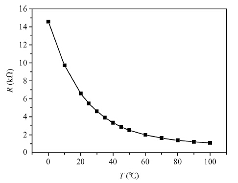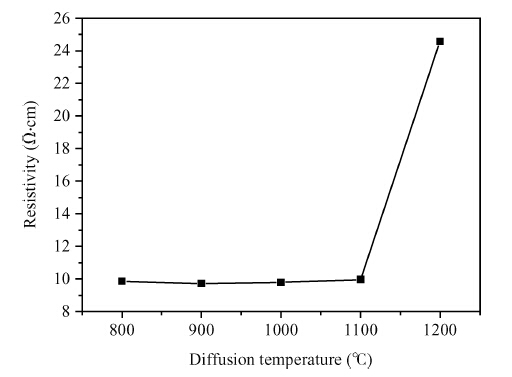
Fig. 1.
Curve of resistivity at different diffusion temperatures.
SEMICONDUCTOR MATERIALS
Yanwei Fan1, 2, Bukang Zhou1, 2, Junhua Wang1, Zhaoyang Chen1 and Aimin Chang1,
Corresponding author: Aimin Chang, E-mail: Changam@ms.xjb.ac.cn
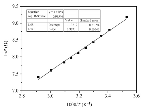
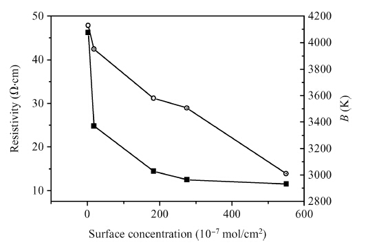
Abstract: Copper doped n-type single-crystal silicon materials are prepared by a high temperature diffusion process. The electrical and thermal-sensitive characteristic of materials is investigated under different experimental conditions. The results show that the maximum resistivity of 46.2 Ω ·cm is obtained when the sample is treated at 1200 ℃ for 2 h with the surface concentration of the copper dopant source being 1.83 × 10⁻⁷ mol/cm2. The copper doped n-type silicon material presents a negative temperature-sensitive characteristic and the B values are about 3010-4130 K.
Keywords: single-crystal silicon, deep level impurity, copper
| [1] | |
| [2] | |
| [3] | |
| [4] | |
| [5] | |
| [6] | |
| [7] | |
| [8] | |
| [9] | |
| [10] | |
| [11] | |
| [12] | |
| [13] | |
| [14] | |
| [15] | |
| [16] | |
| [17] | |
| [18] | |
| [19] |
| [1] | |
| [2] | |
| [3] | |
| [4] | |
| [5] | |
| [6] | |
| [7] | |
| [8] | |
| [9] | |
| [10] | |
| [11] | |
| [12] | |
| [13] | |
| [14] | |
| [15] | |
| [16] | |
| [17] | |
| [18] | |
| [19] |


Article views: 2976 Times PDF downloads: 23 Times Cited by: 0 Times
Received: 13 April 2014 Revised: Online: Published: 01 January 2015
| Citation: |
Yanwei Fan, Bukang Zhou, Junhua Wang, Zhaoyang Chen, Aimin Chang. Preparation and thermal-sensitive characteristic of copper doped n-type silicon material[J]. Journal of Semiconductors, 2015, 36(1): 013004. doi: 10.1088/1674-4926/36/1/013004
****
Y W Fan, B K Zhou, J H Wang, Z Y Chen, A M Chang. Preparation and thermal-sensitive characteristic of copper doped n-type silicon material[J]. J. Semicond., 2015, 36(1): 013004. doi: 10.1088/1674-4926/36/1/013004.

|
| [1] | |
| [2] | |
| [3] | |
| [4] | |
| [5] | |
| [6] | |
| [7] | |
| [8] | |
| [9] | |
| [10] | |
| [11] | |
| [12] | |
| [13] | |
| [14] | |
| [15] | |
| [16] | |
| [17] | |
| [18] | |
| [19] |

 WeChat ID
Journal of Semiconductors © 2017 All Rights Reserved 京ICP备05085259号-2

 DownLoad: