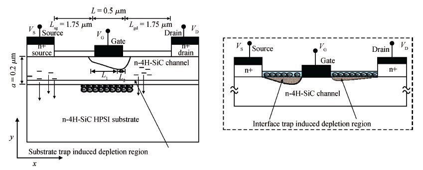
Loading [MathJax]/jax/output/HTML-CSS/jax.js
J. Semicond. > 2015, Volume 36 > Issue 1 > 014004

SEMICONDUCTOR DEVICES

An improved analytical model of 4H-SiC MESFET incorporating bulk and interface trapping effects

M. Hema Lata Rao and N. V. L. Narasimha Murty

+ Author Affiliations

 Corresponding author: M. Hema Lata Rao, E-mail: hlm10@iitbbs.ac.in; N. V. L. Narasimha Murty, E-mail: murtyn@iitbbs.ac.in

DOI: 10.1088/1674-4926/36/1/014004

PDF

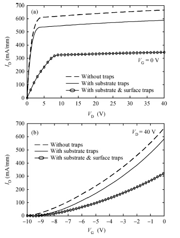
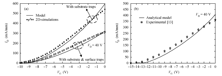
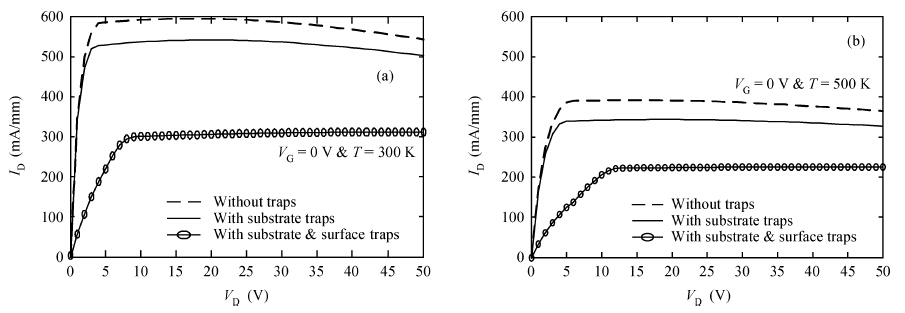
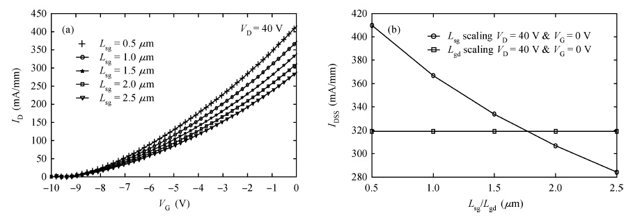
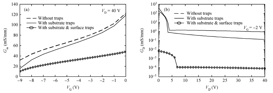
Abstract: An improved analytical model for the current-voltage (I-V) characteristics of the 4H-SiC metal semiconductor field effect transistor (MESFET) on a high purity semi-insulating (HPSI) substrate with trapping and thermal effects is presented. The 4H-SiC MESFET structure includes a stack of HPSI substrates and a uniformly doped channel layer. The trapping effects include both the effect of multiple deep-level traps in the substrate and surface traps between the gate to source/drain. The self-heating effects are also incorporated to obtain the accurate and realistic nature of the analytical model. The importance of the proposed model is emphasised through the inclusion of the recent and exact nature of the traps in the 4H-SiC HPSI substrate responsible for substrate compensation. The analytical model is used to exhibit DC I-V characteristics of the device with and without trapping and thermal effects. From the results, the current degradation is observed due to the surface and substrate trapping effects and the negative conductance introduced by the self-heating effect at a high drain voltage. The calculated results are compared with reported experimental and two-dimensional simulations (Silvaco®-TCAD). The proposed model also illustrates the effectiveness of the gate-source distance scaling effect compared to the gate-drain scaling effect in optimizing 4H-SiC MESFET performance. Results demonstrate that the proposed I-V model of 4H-SiC MESFET is suitable for realizing SiC based monolithic circuits (MMICs) on HPSI substrates.

Key words: SiC MESFETHPSI substratedeep-level trapsMMICs

SiC material has potential applications in high power microwave devices and RF circuitry because of its large bandgap, high saturated electron velocity, high breakdown field and large thermal conductivity[1, 2, 3]. The development of a microwave device such as MESFET, fabricated from 4H polytype of SiC, is of great interest because of its simple construction and wide use in circuit applications namely power amplifiers, mixers and oscillators[4]. The intrinsic material properties of 4H-SiC can be taken as an advantage to construct microwave devices (MESFETs) if the 4H-SiC substrate formed is semi-insulating (SI)[5]. SI substrates are needed to minimize parasitic device capacitances, which in turn reduce the RF losses so that the devices can have enhanced performance at high frequencies. One traditional way of achieving this SI property in 4H-SiC is by introducing transition metals such as vanadium (V). The resulting material is found to be SI at room temperature and retains its nature even at elevated temperatures[6]. However, later reports[5, 7] suggest that V may not be the favorable deep-level trap for SI 4H-SiC. An unacceptably high concentration of V (1017 cm3) in the substrate is used to compensate for the residual shallow acceptors (1016 cm3), which degrade the crystalline and electronic quality of the material by introducing growth defects[8, 9]. Alternatively, compensation of SiC substrates without intentional V doping is explored[10, 11]. Unlike the earlier compensation technique, the intrinsic defects that have energy levels deep in the bandgap (with concentration in the mid 1015 cm3) are used to compensate for the shallow levels, making the substrate semi-insulating[8]. Impressive DC and RF performances of 4H-SiC MESFET formed on 4H-SiC HPSI substrate are demonstrated[12, 13]. Other ways of forming a SI SiC layer in n-type 4H-SiC wafers such as by controlled electron irradiation[14] and by defect competition epitaxy[15] }$ are also reported. The recent developments in the formation of HPSI substrates make SiC MESFET even more attractive for monolithic microwave integrated circuit (MMIC) technology but the device performance is still affected by the trapping centers in the substrate and at the surface of the device[16]. On the other hand, suppression of trapping effects in SiC MESFETs is investigated by separating the conducting channel from the SI substrate by sandwiching a low-doped buffer layer[16]. However, it has been reported that the substrate trapping effects still persist even with buffer layers[16]. Hence it is worthwhile investigating the trapping effects in 4H-SiC MESFETs fabricated directly on HPSI substrates. In addition to the trapping near to the substrate, trapping at the channel-passivation layer interface also affects the microwave performance of the device[17]. The trapping of charge carriers by the surface states present between source/drain, and the gate modulates the channel current and degrades the DC and RF performance of the device. In 4H-SiC MESFETs, trapping effects introduce current collapse in the I-V characteristics, frequency dispersion of transconductance and output resistance, drain and gate lag that severely limits the microwave power output[16, 18, 19]. A physics-based analytical model of 4H-SiC MESFETs including the major trapping effects is crucial for an exact evaluation of device performance at low frequency and microwave applications. Furthermore, it is useful for subsequent optimization once the model is validated.

Tsap[20] presented an analytical I-V model of SiC MESFET including the field-dependent mobility and computed the cut-off frequency of the MESFET. Murray and Roenkar[21] reported a physics-based analytical model of SiC MESFETs based on the two-dimensional analysis of the charge distribution under the gate including the field dependent mobility and velocity saturation effects. In Reference [22], Mukherjee \textit{et al. }presented an analytical model of SiC MESFET with trapping and thermal effects but the exact nature and origin of the traps are not discussed. Zhu et al.[23] reported a three-region model for short channel SiC MESFETs. Chattopadhyay et al.[24] proposed an analytical model of an ion-implanted 4H-SiC MESFET by considering different ion-implantation parameters. A comprehensive frequency dispersion model of 4H-SiC MESFET was proposed by Lu et al.[25]. The small-signal parameters of the MESFET are computed from the modeled DC I-V characteristics. It is observed that the aforementioned models do not consider the effects of both substrate and surface trapping and the actual nature of the HPSI substrate in modeling the DC characteristics of the 4H-SiC MESFET.

The main objective of this paper is to provide an improved analytical model with the recently reported nature and origin of the deep-level traps[10, 11] in the substrate bulk of 4H-SiC MESFET along with the surface trapping effect so that the modeled I-V characteristics can show a closer resemblance to the real devices. The contribution of each trap is validated through two-dimensional simulations (SILVACO®-TCAD)[26]. The surface trapping effect is included through the modulation of parasitic series resistance obtained at the gate-source spacing, as well as the gate-drain spacing of MESFET. For the completeness, self-heating effects are also considered. At present, our model is simulated for DC characteristics. In addition, the transconductance and the drain conductance are determined for the same device. Some of the assumptions considered in the model are also validated by performing two-dimensional device simulations[26] (SILVACO®-TCAD) on the same device.

The schematic structure of 4H-SiC MESFET is shown in Figure 1. A uniform doping concentration (Nd) is assumed throughout the channel of the device approximating the ion-implantation profile considered in experimental results[12]. Here W, L, Lsg, Lgd and a are the gate width, gate length, source-gate spacing, gate-drain spacing and active layer thickness respectively. The device is assumed to be passivated on the ungated regions between source-gate and gate-drain of the device with an insulator, typically silicon dioxide (SiO2). The substrate considered here is an HPSI substrate where the compensation is by deep levels created by intrinsic defects formed during the growth[10]. In Figure 1, the depletion region under the gate is due to the conventional metal-semiconductor junction. Whereas, the depletion region at the channel-substrate interface is due to the capture of energetic channel electrons by the uncompensated deep levels in the substrate, increasing the effective negative charge leading to a positive depletion region in the channel side of the channel-substrate interface (as shown in Figure 1). Similarly, interface states present at the ungated portions between the source and gate as well as between the gate and drain of the 4H-SiC MESFET create a surface depletion region, which is also modulated by the gate and drain voltages leading to voltage dependent series resistance. The inset of Figure 1 demonstrates the surface trapping effects at the channel-dielectric interface. The result of both these effects is the reduction in the drain current under static conditions. The other effects include frequency dispersion of transconductance and output resistance, drain and gate lag that severely limits the microwave power output; however, these effects will be visible when a transient signal is applied to the terminals of the device. In the following sub-sections, modeling of the substrate and surface trapping effects are discussed and later a complete DC I-V model of 4H-SiC MESFET is presented.

Figure  1.  Schematic cross section of a 4H-SiC MESFET. Both substrate and interface trap (inset) induced depletion regions are shown.

For analytical modeling of the substrate trapping effects in 4H-SiC MESFETs, it is essential to identify the dominant defects (traps) that are responsible for substrate compensation and trapping. A multitude of defects in 4H-SiC covering the whole range of energies in the bandgap are reported[27]. However, the intrinsic traps with energy levels ranging from 0.5 to 1.5 eV from the conduction band are found to be responsible for the substrate compensation in 4H-SiC[10]. Out of many intrinsic levels, three major deep-level traps (Z1/2, RD1/2, EH6/7) found in the 4H-SiC substrate are believed to compensate shallow donors and acceptors from residual shallow impurities[10]. The origin of these traps is mainly due to the carbon vacancy, which was revealed by recent electron paramagnetic resonance studies (EPR)[28]. The observation in Reference [10] indicates that these traps are found in the upper half of the bandgap and are acceptor-like. The recent report by Son et al.[29] indicates that Z1/2 is a double acceptor and EH6/7 is a single donor trap.

Table 1 summarizes the typical concentrations and captured cross sections of these three dominant traps in the HPSI substrate used in our analysis. The trap parameters for Z1/2 and RD1/2 are taken from Reference [10], whereas the trap parameters of EH6/7 in the HPSI 4H-SiC substrate are not yet reported. It is observed that the Z1/2 center is always present along with the EH6/7 trap, suggesting that both may be due to C-vacancy related defects in 4H-SiC[29]. Moreover, the concentrations of both traps were found to be very close to each other (with a slightly higher Z1/2 concentration, but of the same order) irrespective of the growth and annealing conditions[29, 30]. Hence, it is reasonable to consider the EH6/7 concentration of the order of 1015 cm3 in HPSI 4H-SiC substrates. We have found that the Fermi level position in the substrate is relatively insensitive to the variation in EH6/7 concentration (changes only by few meV for a decade of change).

Table  1.  Deep level traps in the HPSI substrate of 4H-SiC MESFET with their position, concentration and capture cross sections[10, 30].
DownLoad: CSV  | Show Table

In the subsequent analysis, we have considered the above mentioned three dominant deep-level traps with energies and concentrations specified in Table 1. Many experimental results revealed that nitrogen (EC - 0.090 eV) and Boron (EV + 0.22 eV) are the dominant shallow donors and acceptors with concentrations in the mid 1015 cm3 in HPSI substrates and that nitrogen concentration exceeds the boron concentration[5, 10, 15]. In the analysis, we have assumed the net donor concentration as 2 × 1015 cm3 similar to Mitchel's report[10].

To verify the compensation mechanism in the 4H-SiC HPSI substrate, we have determined the position of the Fermi level in the substrate at thermal equilibrium by applying a charge neutrality condition to the multiple-trap model. Considering the charge states of acceptor and donor-like deep-level traps, incomplete ionization of shallow dopants, the charge neutrality condition can be written as:

n0+NT1+NSA+NT2=p0+N+SD+N+T3,(1)
where n0 is the free electron concentration, p0 is the free hole concentration, N+SD is the ionized shallow donor concentration, NSA is the ionized shallow acceptor concentration, and NT1, NT2, and N+T3 are the densities of ionized Z1/2 (acceptor), RD1/2 (acceptor) and EH6/7 (donor) trap concentrations respectively.

In HPSI 4H-SiC, the Fermi level is in the forbidden bandgap and is several kT away from the band edges and hence Maxwellian statistics are applicable.

The free electron/hole concentrations are given by n0=gNce(EcEf)kT and p0=(Nvg)e(EfEv)kT respectively, where Nc and Nv are the effective density of states in the conduction and valence bands of 4H-SiC[10] and the degeneracy factor (g) of donors and donor-like traps is taken as being two, whereas for acceptor and acceptor-like traps, it is considered as being four[31]. The ionized trap densities NT1, NT2 and N+T3 are given by

NT1(eql)=NZ1/2fT(eql)=NZ1/2(1+1geEZ1/2EfkT)1,(2)
NT2(eql)=NRD1/2fT(eql)=NRD1/2(1+1geERD1/2EfkT)1,(3)
N+T3(eql)=NEH6/7(1fT(eql))=NEH6/7(1+geEfEEH6/7kT)1,(4)
where fT(eql) is the probability of a trap level being occupied by an electron in the substrate under thermal equilibrium. NZ1/2, NRD1/2 and NEH6/7 are the densities of Z1/2, RD1/2 and EH6/7 traps with the energy levels represented by EZ1/2, ERD1/2 and EEH6/7 respectively. Ef is the Fermi energy level in the substrate bulk at thermal equilibrium.

The position of Fermi level can now be determined graphically by plotting each term in Equation (1) as a function of energy (Ef). The above mentioned graphical method is demonstrated in Figure 2 with the reported SIMS results for shallow dopant concentrations[5, 10, 15] and the deep level trap parameters in Table 1. The Fermi level is found to be located at 0.845 eV from the conduction band in the HPSI substrate at thermal equilibrium. The electrons from the shallow donor level can compensate for the lowest acceptor level (near to the valence band), the boron level in this case, first and then the next higher levels (EH6/7, RD1/2 and Z1/2) will be compensated for. Finally, the Fermi level is pinned close to the highest partially compensated deep level, Z1/2 in this case. The resultant material is found to be slightly n-type with a carrier concentration of about 106 cm3. Using the reported electron mobility values of 1-100 cm2/(Vs) for HPSI 4H-SiC[32], the room temperature resistivity is found to be > 1011 Ωcm. The resistivity obtained from the above calculations is comparable to the resistivity of commercially available HPSI 4H-SiC wafers[5, 14, 15], which further confirms that multiple deep-level traps with concentrations of more than 1015 cm3 compensate for the HPSI 4H-SiC substrate.

Figure  2.  Calculated charge density curves for shallow dopants and deep-levels for HPSI 4H-SiC substrate. The Fermi level is found to be at 0.845 eV below the conduction band minimum (EC).

It is evident from the above calculations and the reported experimental results that Z1/2, RD1/2 and EH6/7 traps may be the dominant traps responsible for substrate compensation in 4H-SiC. For modeling and analyzing the substrate trapping effects, it may be helpful in identifying the roles of individual traps towards the overall trapping. To understand this, we have performed two-dimensional device simulations, with commercial simulators[26], of 4H-SiC MESFET having a gate length of 0.5 μm formed directly on the HPSI substrate as in Figure 1. The substrate is modeled initially as trap-free with only the background dopant concentrations and later deep-level traps are introduced with the trap parameters in Table 1. The simulated electron concentration profiles in different regions of the MESFET operating at 300 K are shown in Figure 3. The bias voltages used are Vds = 20 V and Vgs = 6 V. Figures 3(a) and 3(b) present the simulated electron concentration in the MESFET on a substrate defined to be trap-free with only the background doping concentration and with a substrate that contains the three dominant traps. As evident from the figures, the presence of all the traps in the substrate inhibits the electron movement from the channel to the bulk of the substrate. Rather, they get trapped by these traps and hence show a reduction in the electron concentration in the substrate. At high gate and drain voltages, the conducting electrons are pushed away from the channel by the high vertical electric field in the channel and enter into the substrate. Since the substrate in Figure 3(a) is defined as trap-free, the injected electrons stay close to the channel-substrate interface without being trapped, whereas in Figure 3(b), the substrate includes the dominant deep level traps and hence a reduction in the injected electron concentration is observed. These simulations clearly show that trapping effects are present in 4H-SiC MESFETs fabricated on HPSI substrates.

Figure  3.  (Color online) Simulated electron concentration contours to show the drain current injection into the substrate of 4H SiC MESFET at 300 K. The simulation was performed for VG = 6 V and VD = 20 V considering (a) trap-free substrate with only the shallow dopants and (b) substrate with the major deep-level traps along with the shallow dopants.

To further clarify the same, Figure 4 shows the simulated vertical electric field in the substrate along the cutline AA1 of the MESFET structure shown in Figures 3(a) and 3(b). It is noted that the vertical component of the electric field increases for the substrate with traps due to the possible substrate trapping.

Figure  4.  Simulated vertical electric field profile along the cutline AA1 of the MESFET for the substrate without and with deep-level traps.

Figures 5(a) and 5(b) show the simulated electron density profiles of the MESFET without considering EH6/7 and Z1/2 traps in the SiC substrate. By comparing those profiles with Figure 3(b), it can be observed that when the EH6/7 trap is absent, there is an almost negligible change in the electron concentration profile as compared to the profile when all the traps are present in the substrate. On the other hand, major changes in the electron concentration profiles were noticed when Z1/2 was not considered in the simulations. Similar behavior was observed for the RD1/2 trap (not shown). Hence it may be reasonable to neglect the trapping effects of EH6/7 to the overall substrate trapping, even though it takes part in the substrate compensation. The same can be concluded by looking into Figure 2. The calculated Fermi level at thermal equilibrium in the HPSI 4H-SiC substrate was earlier found to lie at 0.845 eV below the conduction band and hence this level is many kT above the EH6/7 level (1.65 eV below the conduction band), as shown in Figure 2. Under normal conditions, this level is almost filled with electrons and trapping by this level may be negligible. Hence the trapping model is developed considering the substrate trapping by Z1/2 and RD1/2 traps in the HPSI substrate.

Figure  5.  (Color online) Simulated electron concentration contours to show the drain current injection into the substrate of 4H SiC MESFET at 300 K. Considering (a) a substrate with the absence of EH6/7 and (b) a substrate with the absence of the Z1/2 trap.

Under non-equilibrium conditions, the Fermi function in the substrate is given by[33]

fT(noneql)=ep+nCnep+en+nCn+pCp,(5)
where Cp=σpvpth and Cn=σnvnth are the hole and electron capture coefficients; σp and σn are the capture cross sections of holes and electrons; n and p are the free electron and hole concentrations at non-equilibrium conditions; vpth and vnth are the thermal velocities of holes and electrons; and ep and en are the emission rates of holes and electrons from the respective traps.

The concentration of negative charge due to electron trapping by a defect level in the substrate side can be given as follows:

NT(noneql)=NT(fT(noneql)).

(6)

fT(noneql) given in Equation (5) can be simplified by considering the non-equilibrium carrier statistics in the 4H-SiC substrate. In unipolar devices like MESFETs, the injected electron density from the channel is orders of magnitude higher than the equilibrium electron and hole concentrations in the HPSI substrate. Moreover, Z1/2 and RD1/2 traps are in the upper half of the bandgap and hence ep < en. Under these conditions, fT(noneql) for traps Z1/2 and RD1/2 can be computed and is nearly equal to 1. This is expected because of the large number of electrons injected into the substrate and the lower concentration of vacant traps.

The net negative charge acquired by the substrate due to trapping by a single defect level is,

Nsub=NT(noneql)NT(eql).

(7)

Extending this equation to multiple deep-level traps (Z1/2 and RD1/2) by neglecting the inter-trap charge transfer, Equation (7) can be written as

Nsub=2i=1NTifTi(noneql)2i=1NTifTi(eql).

(8)

It has been generally agreed that the surface potential of a free-SiC surface is comparable to that of an un-biased Schottky metal gate due to pinning the Fermi level at the surface by high density surface states[34]. Surface passivation with native SiO2 is proposed to reduce the interface state density, but a two orders of magnitude higher interface state density at the SiC/SiO2 interface compared to the Si/SiO2 interface is reported[35]. The high density of electrically active surface/interface states at SiC/SiO2 is responsible for the undesirable surface trapping effects in MESFETs[23, 36], mobility degradation in MOSFETs and the reduction of current gain in BJTs. Particularly in 4H-SiC MESFET, either with an unpassivated or passivated surface, the surface trapping induced depletion layer extends into the channel between the source-gate and gate-drain (inset of Figure 1) modulating the source and drain parasitic resistances (RS and RD). The surface trapping effects may cause a substantial reduction in the channel current and the transconductance, which eventually degrade the DC and microwave performance of these devices. Various techniques for minimizing the surface trapping problems in 4H-SiC MESFETs have been reported in the literature such as surface treatment by dielectric passivation[17, 34], insertion of MOS gate controlled spacer layers between the surface and the channel, recessed gate structures[37] }$ and by gate-connected field plates[38]. Among those techniques, improved surface treatment by dielectric passivation may be promising for monolithic integration and the surface trapping effects are even more noticeable in planar devices[39]. In order to design optimized circuits using SiC MESFETs, a complete analysis of dc characteristics that includes the surface trapping effects is extremely valuable.

Experimental results[40] on the 4H-SiC/SiO2 interface shows a mean interface trap density of the order of 1012~eV1cm2. To include the effect of interface states, the energy and the temperature dependence of the trap density of interface states (Dit(ET,T)) is considered that facilitates the incorporation of different surface passivation effects on the DC characteristics of the MESFET in the model. The typical extracted Dit profiles of the 4H-SiC/SiO2 interface has shown a nearly flat profile near the middle of the bandgap and an exponential increase near the band edges[41]. Thus the energy and temperature dependent Dit distribution can be modeled as[40, 41]

Dit(ET,T)=Dmidit+DCBedgeite(EcET)σ1+DVBedgeite(ETEv)σ2,(9)
where ET is the surface trap level in the energy bandgap, EC is the conduction band minimum, EV is the valence band maximum, Dmidit is the midgap density of states, DCBedgeit(DVBedgeit) and σ1 (σ2) are the interface state density and the characteristic band tail energy at the conduction (valence) band edges respectively.

In order to use the energy dependent Dit profile for further analysis, the unknown parameters in Equation (9) are extracted from the reported Dit distribution for the 4H-SiC/SiO2 interface[42]. The best fit is observed for the extracted values of unknown parameters with Dmidit = 2 × 10¹¹ eV1cm2, DCBedgeit = 6 × 10¹³ eV1cm2, DVBedgeit = 1 × 10¹² eV1cm2, σ1 = 0.25 eV and σ2 = 0.26 eV.

When the MESFET is unbiased, the acceptor interface states below Ef and above the charge neutral level (CNL), ECNL, are negatively charged. Recent quasi-particle calculations[43] performed on SiC polytypes reveals that in 4H-SiC, the CNL lies 1.4 eV below the conduction band minimum. Assuming the CNL is at 1.4 eV below the conduction band and Ef above ECNL, the interface trapped negative charge density is evaluated as

Qit=qEfECNL[Dit(ET)f(ET)]dET,(10)
where f(ET) is the probability of occupying the acceptor trap at ET by an electron.

By applying the charge balance equation at the interface of 4H-SiC/SiO2 and converting the density of state energies into the surface potential, the width of the surface depletion region can be found using,

qNdWS=|qEfECNL[Dit(ET)f(ET)]dET|,(11)
WS=2εSiCVsbiqNd,(12)
EfECNL=Eg[(ECNLEV)+qVsbi+(ECEf,bulk)],(13)
where WS is the width of the surface depletion region at the source end of the unbiased MESFET, Vsbi is the surface built-in potential, εSiC is the permittivity of 4H-SiC, q is the electron charge, Eg is the bandgap of 4H-SiC, and ECEf,bulk is the relative position of the Fermi level in the channel region of 4H-SiC MESFET that can be determined from the channel doping density.

It has been mentioned earlier that surface trapping by the acceptor interface states at the SiC/SiO2 interface leads to the formation of a surface depletion region between gate-source and gate-drain opening of the SiC MESFET. We assume that the surface effects beneath the Schottky gate are included in the determination of the Schottky barrier height (ϕb). When the MESFET is biased, the depletion layers between gate-source and gate-drain are modulated by the gate bias resulting in additional variable series resistances that are connected to the intrinsic FET. These series resistances are larger compared to GaAs MESFETs with similar geometry and doping concentration because of the low value of electron mobility and high interface state densities in 4H-SiC[3, 17]. Moreover, the extracted source and drain series resistances from the measured S-parameters are strongly dependent on the surface passivation conditions[17]. Hence, an analytical model for the voltage dependent series resistances of a 4H-SiC MESFET considering the different surface passivation effects is valuable for accurate device characterization at DC and microwave frequencies.

The source series resistance (RS) between source and gate opening of the MESFET may be given as

RS(VG)=RC+Rsg(VG),(14)
where RC is the contact resistance of the source metal contact and Rsg(VG) is the voltage-dependent series resistance between gate-source opening.

Considering the linear variation of the potential at the interface between the source and the gate (equivalent to gradual channel approximation as long as the source-gate separation, Lsg, is much longer than the surface depletion layer depth), the depletion layer width from the surface at any point in the gate-source spacing is given by[44],

hs(x)={2εsqNd[Vsbiϕs(x)+V(x)]}1/2,(15)
where Vsbi is the surface built-in potential calculated earlier, while ϕs(x)=VsgLsgx and V(x) are the surface potential in the ungated portion of the channel and the potential in the channel at point x.

The depletion layer thickness at the source and gate edges is respectively,

h0s=hs(0)={2εsqNd[Vsbi+V(0)]}1/2,

(16)

h1s=hs(Lsg)={2εsqNd[VsbiVsg+V(Lsg)]}1/2.

(17)

Following the similar analysis of the modeling of RS proposed for GaAs MESFET[44], the voltage dependent source-gate series resistance can be computed by,

Rsg(VG)=1qNdμ0WLsg0dxahs(x).

(18)

The above equation assumes the linear velocity-field characteristics in the ungated region of the channel. The two-dimensional simulations of the electric field profile in the gate-source spacing of the 4H-SiC MESFET in Figure 1 reveals a typical lateral electric field that is much less than the critical field for velocity saturation (not shown here), which confirms the validity of the above assumption.

A similar analysis is performed to find RD at the ungated portion of the 4H-SiC MESFET drain end by appropriately modifying Equations (16) and (18).

For a biased MESFET, self-heating occurs when electrical energy is converted into thermal energy, increasing the lattice temperature which in turn affects electron mobility, ionization and saturation velocity[45, 46]. SiC MESFETs operating at higher drain voltage and current leads to the decrement of mobility and saturation velocity, which ultimately reduces the drain current. The effect is more prominent at larger gate and drain voltages due to the high level of heat dissipation.

The self-heating effect incorporates the influence of temperature through the low-field mobility, the saturation velocity and the free carrier concentration of the device. The reduction of drain current is observed as the drain voltage increases. Here an iterative method proposed in Reference [45] is followed to find the I-V characteristics where the current variation is shown by varying the temperature associated with the power dissipation of the 4H-SiC MESFET and drain voltage.

The analytical model of I-V characteristics incorporate the Caughey-Thomas model of field-dependent electron mobility[21], the substrate trapping of electrons by multiple deep-level traps and the two-dimensional analysis of the charge distribution under the gate.

The current at any point `x' in the channel under the Schottky gate including field dependent mobility and the substrate trapping is expressed as[33],

ID=qWn(x)μ(E)E(x)[ah(x)hb(x)],(19)
where E(x) is the lateral field along the channel, n(x) is the channel electron concentration, μ(x) is the field dependent mobility, while h(x) and hb(x) are the depletion layer thicknesses under the metal gate and in the channel side of channel-substrate (CS) interface at a distance x from the source end of the gate. The analytical expressions for h(x) and hb(x) are given by[47],
h(x)={2εsqNd[VbiVgs+V(x)]}1/2,(20)
hb(x)={2εsqNd(NsubNd+Nsub)[Ubi+V(x)]}1/2,(21)
where Vbi and Ubi (Ubi=kTqlnNdnsub) are the built-in potentials of conventional metal-semiconductor and channel-substrate junctions, respectively; nsub is the electron concentration in the 4H-SiC HPSI substrate; and V(x) is the potential along the channel starting from the source end of the gate (x=0). The term [ah(x)hb(x)] in Equation (19) is the effective channel opening.

Solving Equations (19)-(21) along the length of the gate and considering the effect of source and drain series resistances modeled earlier, the I-V characteristics of a 4H-SiC MESFET in the linear region incorporating substrate and surface trapping can be expressed as[22, 47],

ID=YaVP{[VdsID(RS+RD)VP]1/223(U3DU3S)23k11(U31DU31S)},(22)
where VD is the drain bias, and VP and k11 are constants given by,

VP=qNda22εs,k11=(NsubNsub+Nd)1/2,

US=(VbiVgs+IDRSVP)1/2,

Y=qWvsatμ0(NdNsub)vsatL+μ0[VdsID(RS+RD)],

UD=(VbiVgs+VdsIDRDVP)1/2,

U1D=(Ubi+VdsIDRDVP)1/2,U1S=(Ubi+IDRSVP)1/2.

Here UD(US) is the normalized depletion width under the gate at drain (source) and U1D(U1S) is the normalized depletion width in the channel at the CS interface, vsat is the electron saturation velocity, and μ0 is the low-field electron mobility.

Considering the channel length modulation, the channel under the gate is divided into the linear region (L1) and the velocity saturation region (LL1), as shown in Figure 1. The current equation at x=L1 can be given as[22, 47],

ID=Y1aVP[V(L1)IDRSVP23(U3L1U3S)23k11(U31L1U31S)].(23)
where Y1=qWvsatμ0(NdNsub)vsatL1+μ0(V(L1)IDRS), UL1=[VbiVgs+V(L1)VP]1/2, U1L1=[Ubi+V(L1)VP]1/2, where UL1 is the normalized depletion width under the gate at a point where the electron reaches saturation velocity and U1L1 is the normalized depletion width in the channel at the CS interface.

The current equation at x=L1, which corresponds to velocity saturation, can also be given as[21, 47],

ID=qW(NdNsub)vsatγa(1UL1U1L1k11),(24)
where γ is the velocity saturation factor close to unity.

A two-dimensional analysis of Poisson's equation to calculate the potential in the depletion region under the gate can be expressed as[47],

VdsIDRD=V(L1)+2Eca[VbiVgs+V(L1)VP]1/2π×sinhπ(LL1)2a[VbiVgs+V(L1)VP]1/2,(25)
where Ec is the channel electric field corresponding to velocity saturation condition and V(L1) is the potential in the channel at x=L1.

Solving Equations (23)-(25) simultaneously, the drain current can be determined.

The DC transconductance (output conductance) can be computed by differentiating the current equation with respect to the gate voltage (drain voltage).

It is evident from the previously reported literature that substrate and surface traps are the main causes for current degradation of the 4H-SiC MESFET. Though the trapping effects show the major impact on transient characteristics and frequency dispersion of transconductance, at this point of time, we have only depicted the impact on the DC characteristics. It may be noticed from the analytical model that the presence of deep-level traps and interface traps modifies the I-V characteristics of the device. To study the same, the I-V characteristics of the 4H-SiC MESFET structure in Figure 1 are simulated using the model equations with and without trapping effects. Seen in Figure 6(a) are the ID-VD characteristics at VG = 0~V. The nature of the characteristics without trapping effects shows the usual expected behavior of the 4H-SiC MESFET. A significant reduction in the channel current is noticed due to the trapping of channel electrons by the deep-level traps at the channel-substrate interface. A similar behavior is observed in the ID-VG characteristics of the same device plotted in the saturation region for VD = 40 V, as shown in Figure 6(b). The surface trapping effects on the modeled ID-VD and ID-VG characteristics of the 4H-SiC MESFET are also shown in the same figure. The surface traps are included in the model through the modulation of bias-dependent RS and RD by the interface states present at the 4H-SiC/SiO2 interface, as explained in Section 2.2. Figure 6 reveals that the channel current is substantially reduced by the surface trapping and the extent of reduction depends on the surface passivation conditions as well.

Figure  6.  Modeled I-V characteristics of 4H-SiC MESFET without and with trapping effects. (a) ID-VD characteristics for VG = 0 V and (b) ID-VG characteristics for VD = 40 V.

Figure 7 shows the modeled RS-VG characteristics of a 4H-SiC MESFET for two different Dit profiles[42] (stating different surface passivations SP1 and SP2).

Figure  7.  Modeled RS-VG characteristics for 4H-SiC MESFET at VD = 40 V considering two different Dit profiles for the SiO2/4H-SiC interface.

SP1-Dmidit = 2 × 10¹¹ eV1cm2, DCBedgeit = 6 × 10¹³~eV1cm2, DVBedgeit = 1 × 10¹² eV1cm2, σ1 = 0.25~eV.

SP2-Dmidit = 1 × 10¹⁰ eV1cm2, DCBedgeit = 1 × 10¹³ eV1cm2, DVBedgeit = 1 × 10¹² eV1cm2, σ1 = 0.1 eV.

The two surface passivation conditions SP1 and SP2 (passivated using the nitrogen-hydrogen mixed plasma method for SiO2/4H-SiC) are taken for two different samples at different annealing times, one with as-oxidized and the other annealed for 15 min[42], yielding different interface trap densities and hence varied interface passivation conditions. The energy dependent Dit-profile parameters in Equation (7) are extracted from the reported experimental results[42] for SP1 and SP2. The contact resistance value (RC) is calculated in accordance with the typical specific contact resistance values for Ni/4H-SiC ohmic contacts reported[48] (of the order of 105 Ωcm2), which is found to be 10 Ω. The modeled results clearly show that the series resistance (RS) strongly depends on applied bias, similar to GaAs MESFETs[44] as well as on the surface conditions[17]. The nature of series resistance is found to decrease with the increase of gate voltage and for low values of Dit. A similar behavior is observed in case of drain series resistance (RD) (not shown here) but the values are found to be much lower than source series resistance. In addition to the native bulk and interface defects in 4H-SiC, selective doping of the channel region in MESFET by ion-implantation followed by high temperature annealing damages the surface of the active region. For MESFETs, this may lead to enhanced interface trapping and may increase the series resistance of the device, as is evident from the modeled equations.

In Figure 8(a), our analytical model with multiple deep-level traps is compared with the two-dimensional simulations performed using Silvaco$^{\circledR [26]. The substrate in two-dimensional simulations is modeled considering the dominant traps responsible for substrate trapping (Table 1). In addition to the basic Poisson and continuity equations used in the simulator, the key physical models are SRH for generation and recombination, incomplete ionization of impurities and field-dependent mobility models. The two-dimensional MESFET simulation model considers a uniform doping in the channel, which approximates the ion-implanted MESFET[12]. It is found from the figure that our model closely tracks the two-dimensional simulation results with the same device dimensions. The modeled I-V characteristics, including the surface trapping effects, are also shown in the same figure and are validated by comparing with the two-dimensional simulation results. In the two-dimensional simulations, the surface traps are defined following the procedure reported by Deng et al.[36].

Figure 8(b) shows the comparison of calculated results with the reported experimental results[13]. The ID-VG characteristics are obtained for a 0.5 μm MESFET with a 200 μm width and a channel thickness of 0.23 μm. By observing the nature of the characteristics, it is noted that the calculated result shows good agreement with the experimental results.

Figure  8.  Comparison of analytical ID-VG characteristics of 4H-SiC MESFET with substrate trapping and surface trapping effects at VD = 40 V (a) with two-dimensional simulations (Silvaco® TCAD) of (solid lines-analytical model, symbols-2D simulations) and (b) with reported experimental results.

In our model, we incorporated a very thin layer of SiO2 for passivation and assume that the Dit distributions considered for thinner passivated layers are justified. It is reported[49] that the interface charge density (Dit distribution) within the bandgap of 4H-SiC of a MOS structure varies with the oxide thickness, with higher Dit values for thicker oxides. Since passivation layers are relatively thick as compared to gate oxides, for real devices, the surface effects may be more prominent and severe than computed earlier.

The temperature dependence of the modeled ID-VD characteristics of the SiC MESFET including the major trapping and thermal effects is presented in Figure 9 for VG = 0 V and for operating temperatures 300 K and 500 K. At each temperature, the shift in ID-VD is calculated for two cases: one considering only self-heating effects and the other with trapping and self-heating effects. Self-heating effects are found to aid the current reduction and are more prominent for gate-source voltages near to 0 V and for high drain bias, as shown in Figure 9. This is due to the fact that at higher drain and gate voltages, the heat generation is more and hence have a higher influence on device performance.

Figure  9.  I-V characteristics of 4H-SiC MESFET with substrate trapping, surface trapping and self-heating effects for VG = 0 V at (a) T= 300 K and (b) T= 500 K.

Remembering that at higher operating temperatures, small changes in the Dit-profile are reported for 4H-SiC/SiO2 interface[50], due to a lack of concrete experimental data for temperature dependent Dit variations available in the literature, we have assumed slightly lower values of the earlier extracted Dit-values at high temperatures. The values used for simulating the ID-VD at 500 K are Dmidit = 2 × 10¹¹ eV1cm2, DCBedgeit = 4.8 × 10¹³ eV1cm2, DVBedgeit = 1 × 10¹² eV1cm2, σ1 = 0.28 eV and σ2 = 0.28 eV. These values are in the same range as reported for the SiC/SiO2 interface[50] of 4H-SiC MOSFET at the operating temperature of 200 C. A closer observation of Figure 9 reveals that at higher operating temperatures, the trapping effects both at the interface and substrate bulk are found to be less severe. The reason for this type of behavior may be due to the high probability of detrapping of electrons from the traps in the substrate and at the surface at high temperatures.

One of the important consequences of modeling is that once validated against experimental or simulation results, the model can be used to predict the performance of 4H-SiC MESFETs, even before the device fabrication. This information is a valuable tool for device optimization. Russo et al.[51] have studied the geometrical optimization of gate-source scaling (Lsg) effects in AlGaN/GaN HEMTs with the knowledge of peculiar transport characteristics of GaN compared to GaAs/InP through Monte Carlo simulations. Their results suggest that down scaling of source-gate distance (Lsg) can enhance the device performance considerably. Deng et al.[52] have further extended the previous studies[51] to 4H-SiC MESFETs. Through two-dimensional numerical simulations, they have noticed that the Lsg scaling is more effective than the Lgd scaling for the overall improvement of the device DC and microwave performance. Both researchers have attributed the improved characteristics due to Lsg scaling to the increase in the carrier velocity with the electric field in the source-gate spacing of the device. We have also studied the geometrical scaling effects of Lsg and Lgd on the overall DC performance of the device using the modeled equations. In Figure 10(a), the ID-VG characteristics are plotted for the 4H-SiC MESFET of Figure 1 at VD = 40 V by only varying the gate-source spacing (Lsg) and keeping L and Lgd constant. It is observed that the reduction in Lsg improved the DC performance of the device. The improvement of the channel current is due to the reduction in the source-gate series resistance (Rsg), as can be seen from Equation (13). The effect of Lsg(Lgd)-scaling on the saturated drain current IDSS of the 4H-SiC MESFET with L = 0.5 μm biased at VD = 40 V and VG = 0 V is plotted and is shown in Figure 10(b). For plotting the Lsg(Lgd)-scaling effects, Lgd(Lsg) was kept constant at 1.75 μm and the Lsg(Lgd) was varied from 2.5-0.5 μm. It is observed that Lsg scaling greatly increases the drain current whereas Lgd-scaling has nearly no effect on the saturated drain current. This might be because of the weak dependence of Rgd on Lgd in our model. The modeled results are consistent with the earlier reported simulation results[51, 52].

Figure  10.  (a) ID-VG characteristics of 4H-SiC MESFET in saturation region (VD = 40 V) with varying Lsg and for L= 0.5 μm and Lgd = 1.75 μm. (b) Saturated drain current of the 4H-SiC MESFET as a function of gate-source and gate-drain scaling. The device is operated at VG = 0 V and VD = 40 V.

Finally, the effects of substrate and surface trapping on the transconductance (Gm) and drain conductance (GD) of the SiC MESFET that are derived from the DC I-V characteristics are evaluated from the proposed model and are plotted in Figure 11. The observed characteristics are typical of a SiC MESFET. The nature obtained in Figure 11(a) is in accordance with the reported models[21, 22] where it is demonstrated that the transconductance increases with the gate voltage and is fairly independent of the drain voltage in the saturation region. Figure 11(b) shows the drain conductance versus the drain voltage. For the linear region, the drain conductance is high and slowly decreases with the increase in drain voltage and becomes nearly independent at very high drain bias. As seen in the I-V characteristics, the transconductance and conductance also show a decremented behavior when the trapping effects are included. It can be concluded that substrate and surface trapping degrades the transconductance and drain conductance of the device.

Figure  11.  Effect of substrate and surface trapping effects on the (a) modeled transconductance (Gm) of the SiC MESFET operated at VD = 40~V and (b) the modeled drain conductance (GD) of the SiC MESFET operated at VG = 2 V.

In this paper, we have presented an improved analytical I-V model of a 4H-SiC MESFET directly on an HPSI substrate, which includes the analysis with and without trapping and thermal effects. The substrate trapping effect is realized by the inclusion of deep-level traps. We show here that even with HPSI substrates, the trapping effect cannot be neglected. The involvement of the recent and exact nature of the traps in the substrate bulk of the 4H-SiC MESFET gives a clear picture of the realistic nature of the device, which is an important feature of our model. The effects of parasitic series resistances at the source and drain end of the device are also taken into consideration. The effect of interface states is highlighted through the energy and temperature dependent trap density of interface states, making the model valid for any surface conditions. The model is made complete with the inclusion of self-heating effects. The model projects DC I-V characteristics, transconductance and drain conductance of the simulated device. By analyzing the DC characteristics of the device, it is found that there is a significant reduction in drain current due to the substrate and surface trapping effects. The calculated results are in good agreement with reported experimental[13] and two-dimensional simulations (Silvaco®-TCAD). Finally, we conclude that a complete DC analytical model of 4H-SiC MESFET is projected with all major trapping effects and this may be useful for realizing SiC based MMICs on HPSI substrates.


[1]
[2]
[3]
[4]
[5]
[6]
[7]
[8]
[9]
[10]
[11]
[12]
[13]
[14]
[15]
[16]
[17]
[18]
[19]
[20]
[21]
[22]
[23]
[24]
[25]
[26]
[27]
[28]
[29]
[30]
[31]
[32]
[33]
[34]
[35]
[36]
[37]
[38]
[39]
[40]
[41]
[42]
[43]
[44]
[45]
[46]
[47]
[48]
[49]
[50]
[51]
[52]
Fig. 1.  Schematic cross section of a 4H-SiC MESFET. Both substrate and interface trap (inset) induced depletion regions are shown.

Fig. 2.  Calculated charge density curves for shallow dopants and deep-levels for HPSI 4H-SiC substrate. The Fermi level is found to be at 0.845 eV below the conduction band minimum (EC).

Fig. 3.  (Color online) Simulated electron concentration contours to show the drain current injection into the substrate of 4H SiC MESFET at 300 K. The simulation was performed for VG = 6 V and VD = 20 V considering (a) trap-free substrate with only the shallow dopants and (b) substrate with the major deep-level traps along with the shallow dopants.

Fig. 4.  Simulated vertical electric field profile along the cutline AA1 of the MESFET for the substrate without and with deep-level traps.

Fig. 5.  (Color online) Simulated electron concentration contours to show the drain current injection into the substrate of 4H SiC MESFET at 300 K. Considering (a) a substrate with the absence of EH6/7 and (b) a substrate with the absence of the Z1/2 trap.

Fig. 6.  Modeled I-V characteristics of 4H-SiC MESFET without and with trapping effects. (a) ID-VD characteristics for VG = 0 V and (b) ID-VG characteristics for VD = 40 V.

Fig. 7.  Modeled RS-VG characteristics for 4H-SiC MESFET at VD = 40 V considering two different Dit profiles for the SiO2/4H-SiC interface.

Fig. 8.  Comparison of analytical ID-VG characteristics of 4H-SiC MESFET with substrate trapping and surface trapping effects at VD = 40 V (a) with two-dimensional simulations (Silvaco® TCAD) of (solid lines-analytical model, symbols-2D simulations) and (b) with reported experimental results.

Fig. 9.  I-V characteristics of 4H-SiC MESFET with substrate trapping, surface trapping and self-heating effects for VG = 0 V at (a) T= 300 K and (b) T= 500 K.

Fig. 10.  (a) ID-VG characteristics of 4H-SiC MESFET in saturation region (VD = 40 V) with varying Lsg and for L= 0.5 μm and Lgd = 1.75 μm. (b) Saturated drain current of the 4H-SiC MESFET as a function of gate-source and gate-drain scaling. The device is operated at VG = 0 V and VD = 40 V.

Fig. 11.  Effect of substrate and surface trapping effects on the (a) modeled transconductance (Gm) of the SiC MESFET operated at VD = 40~V and (b) the modeled drain conductance (GD) of the SiC MESFET operated at VG = 2 V.

Table 1.   Deep level traps in the HPSI substrate of 4H-SiC MESFET with their position, concentration and capture cross sections[10, 30].

DownLoad: CSV
DownLoad: CSV
DownLoad: CSV
DownLoad: CSV
DownLoad: CSV
DownLoad: CSV
DownLoad: CSV
DownLoad: CSV
DownLoad: CSV
DownLoad: CSV
DownLoad: CSV
DownLoad: CSV
DownLoad: CSV
DownLoad: CSV
DownLoad: CSV
DownLoad: CSV
DownLoad: CSV
DownLoad: CSV
DownLoad: CSV
DownLoad: CSV
[1]
[2]
[3]
[4]
[5]
[6]
[7]
[8]
[9]
[10]
[11]
[12]
[13]
[14]
[15]
[16]
[17]
[18]
[19]
[20]
[21]
[22]
[23]
[24]
[25]
[26]
[27]
[28]
[29]
[30]
[31]
[32]
[33]
[34]
[35]
[36]
[37]
[38]
[39]
[40]
[41]
[42]
[43]
[44]
[45]
[46]
[47]
[48]
[49]
[50]
[51]
[52]
1

Semiconductor steady state defect effective Fermi level and deep level transient spectroscopy depth profiling

Ken K. Chin, Zimeng Cheng

Journal of Semiconductors, 2016, 37(9): 092003. doi: 10.1088/1674-4926/37/9/092003

2

A high power active circulator using GaN MMIC power amplifiers

Liming Gu, Wenquan Che, Fan-Hsiu Huang, Hsien-Chin Chiu

Journal of Semiconductors, 2014, 35(11): 115003. doi: 10.1088/1674-4926/35/11/115003

3

A broadband GaAs MMIC frequency doubler on left-handed nonlinear transmission lines

Dong Junrong, Huang Jie, Tian Chao, Yang Hao, Zhang Haiying, et al.

Journal of Semiconductors, 2011, 32(9): 095003. doi: 10.1088/1674-4926/32/9/095003

4

Neutron radiation effect on 4H-SiC MESFETs and SBDs

Zhang Lin, Zhang Yimen, Zhang Yuming, Han Chao

Journal of Semiconductors, 2010, 31(11): 114006. doi: 10.1088/1674-4926/31/11/114006

5

Improved dual-channel 4H-SiC MESFETs with high doped n-type surface layers and step-gate structure

Deng Xiaochuan, Zhang Bo, Li Zhaoji, Zhang Yourun

Journal of Semiconductors, 2009, 30(7): 074001. doi: 10.1088/1674-4926/30/7/074001

6

Microwave frequency detector at X-band using GaAs MMIC technology

Zhang Jun, Liao Xiaoping, Jiao Yongchang

Journal of Semiconductors, 2009, 30(4): 044009. doi: 10.1088/1674-4926/30/4/044009

7

MMIC-Based RF On-Chip LC Passive Filters

Wu Rui, Liao Xiaoping, Zhang Zhiqiang

Journal of Semiconductors, 2008, 29(12): 2437-2442.

8

A 12~18GHz Wide Band VCO Based on Quasi-MMIC

Wang Shaodong, Gao Xuebang, Wu Hongjiang, Wang Xiangwei, Mo Lidong, et al.

Journal of Semiconductors, 2008, 29(1): 63-68.

9

14W X-Band AlGaN/GaN HEMT Power MMICs

Chen Tangsheng, Zhang Bin, Ren Chunjiang, Jiao Gang, Zheng Weibin, et al.

Journal of Semiconductors, 2008, 29(6): 1027-1030.

10

Influence of the Trapping Effect on Temperature Characteristics in 4H-SiC MESFETs

Lü Hongliang, Zhang Yimen, Zhang Yuming, Che Yong, Wang Yuehu, et al.

Journal of Semiconductors, 2008, 29(2): 334-337.

11

A Simple Method of Surface Parameter Extraction for Gate Schottky Contact in 4H-SiC MESFETs

Lü Hongliang, Zhang Yimen, Zhang Yuming, Che Yong, Sun Ming, et al.

Journal of Semiconductors, 2008, 29(3): 458-460.

12

Characterization and Reliability of Thin Film Resistors for MMICs Application Based on AlGaN/GaN HEMTs

Yao Xiaojiang, Pu Yan, Liu Xinyu, Wu Weichao

Journal of Semiconductors, 2008, 29(7): 1246-1248.

13

1.0μm Gate-Length GaAs MHEMT Devices and SPDT Switch MMICs

Xu Jingbo, Li Ming, Zhang Haiying, Wang Wenxin, Yin Junjian, et al.

Journal of Semiconductors, 2008, 29(4): 668-671.

14

A New Empirical Large Signal Model of 4H-SiC MESFETs for the Nonlinear Analysis

Cao Quanjun, Zhang Yimen, Zhang Yuming, Lü Hongliang, Guo Hui, et al.

Chinese Journal of Semiconductors , 2007, 28(7): 1023-1029.

15

Fabrication of SiC MESFETs for Microwave Power Applications

Bai Song, Chen Gang, Zhang Tao, Li Zheyang, Wang Hao, et al.

Chinese Journal of Semiconductors , 2007, 28(1): 10-13.

16

Epitaxial Growth of 4H-SiC MESFET Structures

Li Zheyang, Dong Xun, Bai Song, Chen Gang, Chen Tangsheng, et al.

Chinese Journal of Semiconductors , 2007, 28(S1): 379-381.

17

4H-SiC MESFET Device Process

Chen Gang, Bai Song, Zhang Tao, Wang Hao, Li Zheyang, et al.

Chinese Journal of Semiconductors , 2007, 28(S1): 565-567.

18

S-Band 1mm SiC MESFET with 2W Output on Semi-Insulated SiC Substrate

Cai Shujun, Pan Hongshu, Chen Hao, Li Liang, Zhao Zhenping, et al.

Chinese Journal of Semiconductors , 2006, 27(2): 266-269.

19

Passive Component Models for GaAs MMICs

Shen Huajun, Chen Yanhu, Yan Beiping, Yang Wei, Ge Ji, et al.

Chinese Journal of Semiconductors , 2006, 27(10): 1872-1879.

20

Microwave Power-Tested Technology of SiC MESFET

Wang Tongxiang, Pan Hongshu, Li Liang

Chinese Journal of Semiconductors , 2006, 27(S1): 239-241.

1. Ali, A., Ali, A., Hussain Zahid, A. et al. A non linear model to analyze the DC performance of SiC MESFET. Ain Shams Engineering Journal, 2021. doi:10.1016/j.asej.2021.05.020
2. Li, S., Xu, Z., Wei, J. et al. Investigation of radiation influences on electrical parameters of 4H-SiC VDMOS | [辐照对4H-SiC VDMOS电学参数的影响]. Journal of Southeast University (English Edition), 2018, 34(4): 474-479. doi:10.3969/j.issn.1003-7985.2018.04.009
3. Dutta, S.. Frequency performance of a SiC MESFET with a moderately doped buffer layer. International Journal of Electronics Letters, 2018, 6(1): 58-69. doi:10.1080/21681724.2017.1293168
4. Riaz, M., Ahmed, M.M., Rafique, U. et al. Assessment of intrinsic small signal parameters of submicron SiC MESFETs. Solid-State Electronics, 2018. doi:10.1016/j.sse.2017.10.040
5. Dutta, S.. Impact of parasitic resistances on the electrical characteristics of a SiC MESFET. Superlattices and Microstructures, 2017. doi:10.1016/j.spmi.2017.09.013
6. Dutta, S.. A theoretical study on the linearity of the Id-T curve of a SiC MESFET for sensor application. Superlattices and Microstructures, 2017. doi:10.1016/j.spmi.2016.12.010
7. Yan, G., Feng, Z., Niu, Y. et al. Chloride-based fast homoepitaxial growth of 4H-SiC films in a vertical hot-wall CVD. Journal of Semiconductors, 2016, 37(6): 063001. doi:10.1088/1674-4926/37/6/063001
8. Li, Y., Deng, X., Liu, Y. et al. Effect of post oxidation annealing in nitric oxide on interface properties of 4H-SiC/SiO2 after high temperature oxidation. Journal of Semiconductors, 2015, 36(9): 094003. doi:10.1088/1674-4926/36/9/094003
  • Search

    Advanced Search >>

    GET CITATION

    shu

    Export: BibTex EndNote

    Article Metrics

    Article views: 3342 Times PDF downloads: 46 Times Cited by: 8 Times

    History

    Received: 19 August 2014 Revised: Online: Published: 01 January 2015

    Catalog

      Email This Article

      User name:
      Email:*请输入正确邮箱
      Code:*验证码错误
      M. Hema Lata Rao, N. V. L. Narasimha Murty. An improved analytical model of 4H-SiC MESFET incorporating bulk and interface trapping effects[J]. Journal of Semiconductors, 2015, 36(1): 014004. doi: 10.1088/1674-4926/36/1/014004 ****M. H. L. Rao, N. V. L. N. Murty. An improved analytical model of 4H-SiC MESFET incorporating bulk and interface trapping effects[J]. J. Semicond., 2015, 36(1): 014004. doi:  10.1088/1674-4926/36/1/014004.
      Citation:
      M. Hema Lata Rao, N. V. L. Narasimha Murty. An improved analytical model of 4H-SiC MESFET incorporating bulk and interface trapping effects[J]. Journal of Semiconductors, 2015, 36(1): 014004. doi: 10.1088/1674-4926/36/1/014004 ****
      M. H. L. Rao, N. V. L. N. Murty. An improved analytical model of 4H-SiC MESFET incorporating bulk and interface trapping effects[J]. J. Semicond., 2015, 36(1): 014004. doi:  10.1088/1674-4926/36/1/014004.

      An improved analytical model of 4H-SiC MESFET incorporating bulk and interface trapping effects

      DOI: 10.1088/1674-4926/36/1/014004
      More Information
      • Corresponding author: E-mail: hlm10@iitbbs.ac.in; E-mail: murtyn@iitbbs.ac.in
      • Received Date: 2014-08-19
      • Published Date: 2015-01-25

      Catalog

        /

        DownLoad:  Full-Size Img  PowerPoint
        Return
        Return