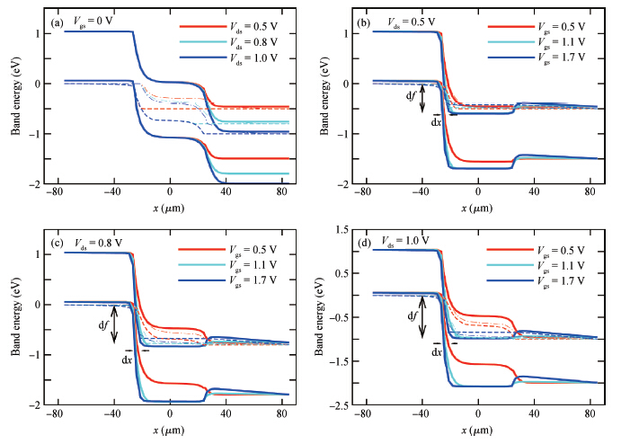
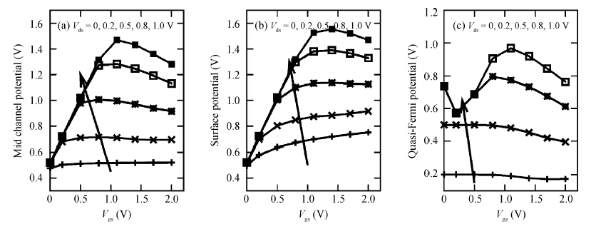
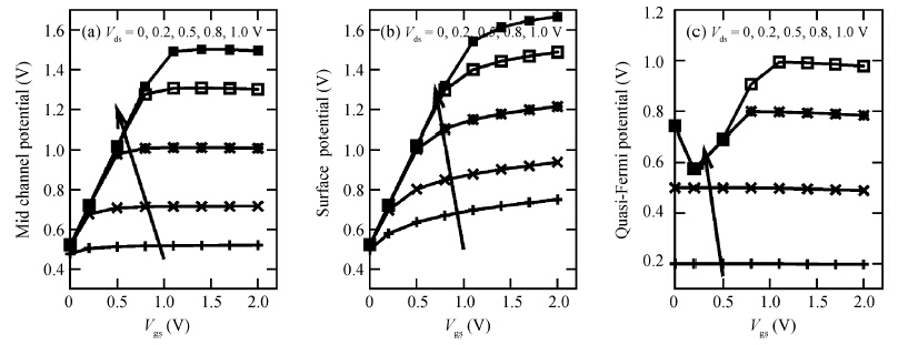
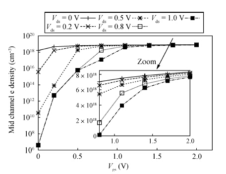
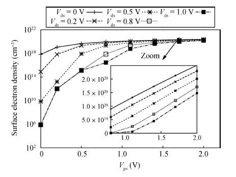
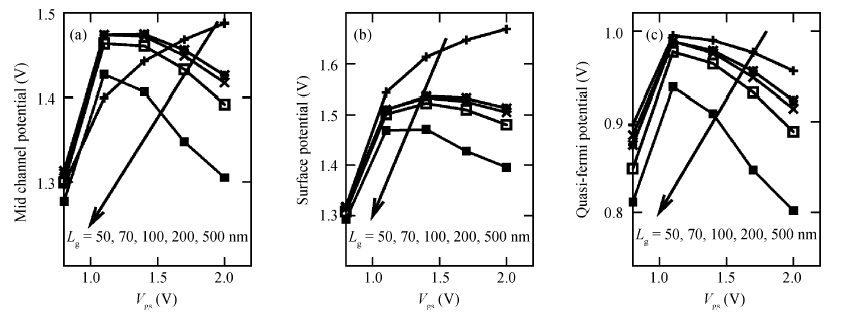
Abstract: A detailed investigation carried out, with the help of extensive simulations using the TCAD device simulator Sentaurus, with the aim of achieving an understanding of the effects of variations in gate and drain potentials on the device characteristics of a silicon double-gate tunnel field effect transistor (Si-DG TFET) is reported in this paper. The investigation is mainly aimed at studying electrical properties such as the electric potential, the electron density, and the electron quasi-Fermi potential in a channel. From the simulation results, it is found that the electrical properties in the channel region of the DG TFET are different from those for a DG MOSFET. It is observed that the central channel potential of the DG TFET is not pinned to a fixed potential even after the threshold is passed (as in the case of the DG MOSFET); instead, it initially increases and later on decreases with increasing gate voltage, and this is also the behavior exhibited by the surface potential of the device. However, the drain current always increases with the applied gate voltage. It is also observed that the electron quasi-Fermi potential (eQFP) decreases as the channel potential starts to decrease, and there are hiphops in the channel eQFP for higher applied drain voltages. The channel regime resistance is also observed for higher gate length, which has a great effect on the I-V characteristics of the DG TFET device. These channel regime electrical properties will be very useful for determining the tunneling current; thus these results may have further uses in developing analytical current models.
Keywords:
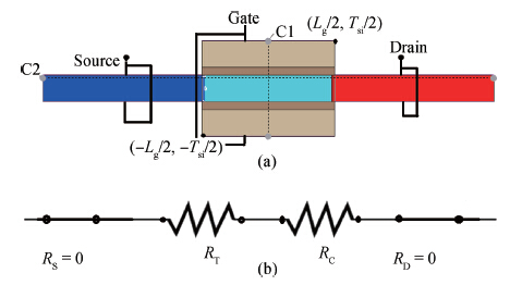
Si-DG TFET, electron quasi-Fermi potential, I-V characteristics, drain extension regime resistance, resistive drop, channel properties


 DownLoad: