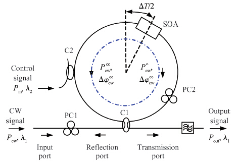
J. Semicond. > 2015, Volume 36 > Issue 1 > 014013

SEMICONDUCTOR DEVICES

All-optical NRZ wavelength conversion using a Sagnac loop with optimized SOA characteristics

Xiyan Jiang, Jin Wang, Chen Gao, Ji Xu and Hongdan Wan

+ Author Affiliations

 Corresponding author: Jin Wang, E-mail: jinwang@njupt.edu.cn

DOI: 10.1088/1674-4926/36/1/014013

PDF

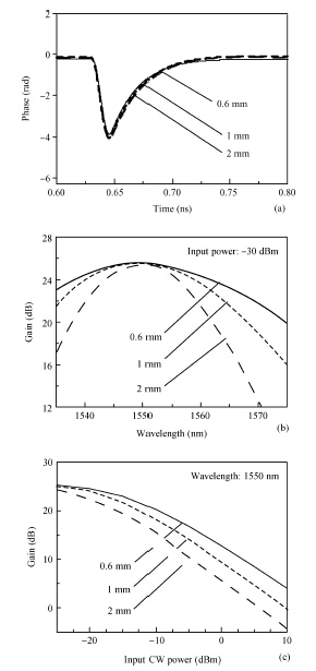
Abstract: We investigated the all-optical wavelength conversion technique for non-return-to-zero (NRZ) signals based on a Sagnac loop interferometer using an SOA. For the wavelength conversion of the NRZ signal at and above 40 Gbit/s, we used an in-house numerical SOA model to analyze the influence of the SOA carrier characteristics and the SOA length on the performance of the Sagnac loop. We found that the SOA carrier recovery time should be between 2 and 3 times of one bit duration in order to get optimum NRZ wavelength conversion. In addition to the carrier recovery time requirement, SOAs with a shorter physical length are preferred to be used in the Sagnac interferometer.

Key words: semiconductor optical amplifierwavelength conversionnon-return-to-zero signalcross-gain modulationcross-phase modulation

All-optical wavelength converters (AOWCs) based on semiconductor optical amplifiers (SOAs) make possible reuse of the local wavelengths and are well suited to overcome wavelength blocking issues in next generation transparent networks. Several interferometric schemes to realize AOWC have been proposed[1, 2, 3, 4, 5]. These schemes have the advantage of very steep transfer functions leading to principally ideal extinction ratios[2], very high-speed operation at, for example, 320 Gb/s[3], and reconfigurable logic operation[5].

While most wavelength conversion experiments employ a return-to-zero (RZ) format, there are only few schemes that allow operation with the non-return-to-zero (NRZ) format[6, 7, 8]. Yet, the NRZ format has gained interest due to the simplicity of this transmission format, its reasonable dispersion tolerance, and its spectral efficiency. One of the few schemes that allows for regenerative operation with NRZ format is the SOA-based Sagnac interferometer scheme, also called SLALOM[1], which has been successfully demonstrated up to 42.7 Gb/s[7].

Operating with an SOA in a Sagnac interferometer offers one advantage: the SOA can operate at a relatively slow speed. This happens because the output signal power is proportional to the integral over the input signal power, and the high-frequency noise is washed out. However, a good performance is only obtained if an SOA with proper physical characteristics, such as cross-gain modulation (XGM) and cross-phase modulation (XPM), is selected. Indeed, the influence of the SOA characteristics, especially the SOA carrier recovery time, on the performance of the wavelength conversion with a Sagnac interferometer has not been well understood.

In this work, we investigated how the operation speed of the NRZ wavelength conversion and the SOA carrier dynamics were related. Since the fabrication of SOAs with desired carrier dynamics was difficult, the investigation was done via simulations using an in-house numerical SOA model[8]. We found that for a particular operation speed the SOA recovery process should neither be too fast nor be too slow. Precisely, the optimum carrier recovery time is between 2 and 3 times of one bit duration. Besides, SOAs with a shorter physical length are preferred to be used in the Sagnac interferometer.

The wavelength conversion scheme using a Sagnac interferometer is shown in Figure 1. An SOA is asymmetrically arranged in the Sagnac loop, which is offset by a time delay ΔT/2 away from the center of the Sagnac loop. A coupler C1 splits a continuous wave (CW) signal with wavelength λ1 into two counter-propagating CW waves. They are termed as the clockwise propagating wave PcCW with a superscript "c" and the counter-clockwise propagating wave PccCW with a superscript "cc", respectively. Another coupler C2 introduces an input data signal Pin at a wavelength λ2 into the Sagnac loop. This input signal induces nonlinear amplitude phases and nonlinear phase changes (ΔϕcCW and ΔϕccCW) on the two counter-propagating waves through the SOA. The two counter-propagating waves combine in the coupler C1 and form a wavelength converted signal Pout. A polarization controller PC1 is used to control the polarization of the CW signal. Another polarization controller PC2 is added close to the coupler C1, which sets a phase difference ψ between the two counter-propagating waves[6, 9]. The polarization controller PC2 is a birefringent device, usually a waveplate, which has a retardation ϕ and an orientation θ. In the Cartesian coordinate system, the orientation θ is the angle of the fast axis e with respect to the y-polarization direction of the complex field. The retardation ϕ is the phase lead of the field component on the fast axis e with respect to the field component on the slow axis o. Such a waveplate can be described by the Jones matrix[9, 10].

Figure  1.  Wavelength conversion scheme using a Sagnac loop based on SOA.

The operation of this wavelength convertor, that is, how the input power is mapped onto the output, depends on the relative phase difference ΔϕccCWΔϕcCW+ψ between the co- and counter-propagating signals. Figure 2 illuminates a wavelength conversion through a Sagnac loop with a selected SOA (named as SOA2), whose physical properties will be discussed in the next section. With respect to Figure 2, the phase difference should be set such that:

Figure  2.  Wavelength conversion from (a) an input signal to (c) output signals through a Sagnac loop with a selected SOA2. (b) The phase difference of two counter-propagating signals after the SOA2.

(1) When the input signal transits from 01, the phase difference is close to zero, see the time point (I) in Figure 2(b). This ensures that the strongest gain depletion and in turn the largest phase shift induced by the input signal result in the lowest transmitted power, see the solid line at the time point (I) in Figure 2(c). Thus, there is speed-up by the XPM for a transition 10 of the output signal. Since subsequent input bits stay on the high level, that is, multiple bit 1 s, the SOA gets more and more depleted and the device stays switched-off. Meanwhile, the phase difference gradually relaxes back to the initial phase offset ψ, and the device is gradually switched on. However, there is not much power at the output due to the strongly suppressed gain in the SOA, see the time slot between (I) and (II). In short, the device now works mostly in the XGM mode.

(2) When the input signal transits from 10, the phase difference is larger and this switches on the device. As a consequence, most powers from PcCW and PccCW are directed into the transmitted port, thus speeding up the recovery and leading to a transition 01 of the output signal, see the solid line at the time point (II) in Figure 2(c). For a series of 0 s in the input signal thereafter, the SOA relaxes back to the initial carrier density level and the phase difference also relaxes back to the initial phase offset ψ. In this case, part of power from PcCW and PccCW are directed into the reflection port.

In summary, the SOA carrier dynamics, both XGM and XPM effects, influence the performance of the wavelength conversion. The Sagnac interferometer provides speed-up by means of XPM whenever there is a transition 01 or 10, but it operates as a pure XGM device in all other situations when there are long series of 0 s or 1 s in the input signal. The extinction ratio between the bit 0 and 1 of the output signal is ultimately determined by the XGM.

To find the proper SOA carrier dynamics in the wavelength conversion process, we prepared three numerical SOAs having various carrier recovery times. The carrier recovery time was derived schematically from a numerical pump-probe experiment, as shown in Figure 3(a). By applying the numerical SOA model from Reference [8], which has been verified with real SOAs, we prepared the SOA1, SOA2 and SOA3, with 10 : 90 carrier recovery times of 76, 52 and 34 ps, Figure 3(b), but with identical gain spectra, Figure 3(c). The recovery times cited above really were the phase recovery times of the SOAs and not the gain recovery times. The phase recovery is mostly influenced by the band-filling dynamics[8, 9], which is the relevant process at 40 Gbit/s corresponding to a bit duration of 25 ps. The respective SOA recovery times were obtained by varying the differential gain and bias current of a generic SOA. The active region of the SOAs is 1 mm long and the other SOA parameters are given in Appendix B. The CW-probe signal was at 1550 nm with a power level of 5 dBm and the pump pulse was at 1558 nm with a peak power of 14.77~dBm.

Figure  3.  (a) Schematic pump-probe experiment setup. (b) Phase recovery dynamics of three prepared SOAs. (c) Gain spectra. (d) Gain saturation characteristic.

These three SOAs having various carrier recovery times were incorporated into the Sagnac loop. Since the main interest in this work is the influence of the SOA dynamics, the power splitting ratios of the couplers used in the simulation are then fixed. In agreement to those used in a previous experiment[7], the power splitting ratio was chosen to be 50 :~50 for the coupler C1, while 80 : 20 for the coupler C2 (co-propagating signal transmission 80 %, input data signal transmission 20 %). The deviation of these ratios in the respective couplers may modify the requirements on the input powers but do not change the principle of the operation. The input data signal used in the simulation is a NRZ signal at an optical carrier of 1558~nm, which is modulated with a PRBS sequence of 28 -1 at 40~Gbit/s. The input data signal has an average power of 12 dBm and the CW signal has a power level of 3 dBm. The time delay ΔT has been set to 2 ps.

The output signals at 40 Gbit/s from the Sagnac loop using a slower SOA1, a "moderate" fast SOA2, and a faster SOA3 are compared between Figures 2(c) and 4. Note that only snapshots between 0.4 and 1.2 ns are shown. It can be seen that the best wavelength conversion was obtained with "moderate" fast SOA2, which had a carrier recovery time of 2 times of one bit duration. Other observations in Figure 4 are:

Figure  4.  Wavelength converted signals after a Sagnac loop with (a) a "slow" SOA1 and (b) a "fast" SOA3.

(1) When a slow SOA1 was used, the XPM effect was dominant. As the multiple input bit 0 s came in, the slow phase recovery gave a quite constant power level in the transmitted signal; see the solid line after the time point (II) in Figure 4(a). However, if a single input bit 0 came in, for example, corresponding to an output bit 1 (solid line) at the time points (II) and (III) in Figure 4(a), the pattern effect due to the slow carrier recovery dynamics was still the problem.

(2) When a fast SOA3 was used, the XGM effect was dominant. In this case, the pattern effect did not trouble the single output bit 1, see the solid line at the time points (II) and (III) in Figure 4(b). As multiple input bit 0s set in, leading to the output 1 s (solid line) after the time point (II) in Figure 4(b), the phase difference relaxed back much more quickly (with respect to the case using SOA2 or SOA1) to the initial phase offset. As a consequence, more than enough light was guided to the reflection port. As a whole, the output NRZ signal was not well formed.

As a performance judgement, Q-factor improvement between the input data signal and the output wavelength converted signal is evaluated when these prepared SOAs are used. The Q-factor measurement is an effective estimation of the bit-error rate (BER), which requires costly equipment in the practice and which also needs much longer computational time in the simulation. A positive Q-factor improvement (in dB) represents signal regeneration. In our simulation, the input data signal is then a noise-loaded PRBS signal having a constant Q-factor of 15.9 dB. To simulate the real operation environment much closely, an additive noise is included in the output signal via a linear booster amplifier behind the Sagnac loop. The noise figure of this linear booster amplifier is set to be 5~dB. After optimizing the optical powers of the input data signal and the CW signal, a Q-factor improvement of about 1.8~dB is obtained when SOA2 is used in the wavelength, and a Q-factor improvement of about 0.5 dB is obtained for SOA3, while a best Q-factor improvement by using SOA1 is about -0.9 dB.

We have also investigated the influence of the SOA length on the wavelength conversion using a Sagnac loop. As known from Reference [6], the gain and phase saturation characteristics for two counter-propagating waves through an SOA can be considerably different. This happens because the gain saturation and phase shift for the counter-clockwise propagating signal are proportional to the integral over the SOA length[11]. Thus, a Sagnac interferometer may compensate the low-pass characteristics of an SOA with a given length for the co-propagating signal, but not for the counter-propagating one.

To compare the wavelength conversion performance with differently long SOAs, we prepared two more SOAs having an active region length of 0.6 and 2 mm respectively. They were termed as SOA4 and SOA5, respectively, and compared with the SOA2 having an active region length of 1 mm. The carrier recovery times of three SOAs were kept to be 52 ps for same input powers, as seen in Figure 5(a). The same carrier recovery time was achieved by varying the bias current applied according to SOA lengths. However, the gain spectra of these three SOAs were different. In fact, a long SOA can be understood as a cascading of several short SOAs. Thus, as shown in Figure 5(b), the longer the SOA, the narrower the gain spectrum was. In addition, Figure 5(c) compares the gain saturation characteristics of these three SOAs. We can observe that for same saturation levels, a weaker input power was needed for a longer SOA, which was due to a longer nonlinear interaction length.

Figure  5.  Characteristic of SOAs with a length of 0.6 mm, 1 mm and 2 mm. (a) Phase recovery dynamics of three prepared SOAs. (b) Gain spectra. (c) Gain saturation characteristic.

With prepared SOA4 and SOA5, we simulated the wavelength conversion at 40 Gbit/s, where the input data signal had an average power of 14 dBm for SOA4 and 10 dBm for SOA5. The CW power was 3 dBm. The other parameters were unchanged. Our results are shown in Figure 6.

Figure  6.  Wavelength converted signals through the Sagnac loop with an SOA having a length of (a) 0.6 mm or (b) 2 mm.

Comparing the output signals by using SOA2 (Figure 2), SOA4 and SOA5 (Figure 6), the performance by using the shorter SOA4 was better. Indeed, a longer SOA5 was not a good choice for the Sagnac loop based wavelength conversion. The reason for this lies in the asymmetric gain saturation and phase shift of two counter-propagating signals after the SOA. On the one hand, the clockwise propagating signal Pccw co-propagates with the input data signal through the SOA and experiences the XGM and the XPM, which are proportional to the integral over the input data signal[6, 11]. On the other hand, the gain saturation and phase shift for the counter-clockwise propagating signal Pcccw are not only proportional to the integral over the input data signal but are also proportional to the integral over the SOA length[11]. Thus, in a longer SOA the gain saturation for Pcccw affects over a large time scale. For instance, at the time point (IV) in Figure 6(b), as the next pulse came the power gain and the phase shift of Pcccw had not yet recovered. As a consequence, the output power for such a bit was also low, see the solid line at the time point (IV) in Figure 6(b). Note that the time points (IV) for SOA4 and SOA5 in Figure 6 were at different times, which was due to different signal transit times through SOA4 and SOA5.

The Q-factor improvement between the input data signal and the output wavelength converted signal is also evaluated for these two SOAs. By using a shorter SOA4, a Q-factor improvement of about 1.9 dB is obtained, while for a longer SOA5, the best Q-factor improvement is about -1.0 dB. Thus, the shorter SOA is preferred in such wavelength convertors.

In this work, we investigated the wavelength conversion process in the SOA-based Sagnac interferometer, and we especially studied the influence from the SOA carrier dynamics. First of all, we found that the XGM and XPM effects in the SOA should collaborate in a proper way for the NRZ wavelength conversion. The simulation results also revealed that an SOA with a carrier recovery time between 2 and 3 times of one bit duration gives the best output NRZ signal. Besides this carrier recovery time requirement, short SOAs are rather preferred in the Sagnac loop. This observation lies in the fact that material responses experienced by the signals from different directions become symmetric in short SOAs.

Although the operation speeds analyzed in this work were 40 Gbit/s, the criteria of choosing a proper SOA is applicable at higher speed NRZ wavelength conversion based on the Sagnac loop.

To analyze the wavelength conversion process in the SOA-based Sagnac loop, the SOA carrier dynamics and the amplification of the optical signals need to be calculated.

In this work, the carrier dynamics are obtained from solving the rate equation of the total carrier density N. Since charge neutrality is assumed, N accounts for both electrons and holes. In addition, a uniform distribution of the bias current Ibias across the active region width is assumed. Then, the material gain gm at the wavelength λ can be calculated from the linear gain term gl, which is a function of N given in Reference [8], the nonlinear spectral-hole-burning (SHB) gain compression term gβ and the nonlinear carrier-heating (CH) gain compression term gT,β. The carrier rate equation for an SOA with a length L and a cross section area σ of the active region is

Nt=IbiasqσLRtot2vgkgmk(scASE,k+sccASE,k)vg(gmCW+gTPACWΓ)(ScCW+SccCW)vg(gmin+gTPAinΓ)(Scin+Sccin),
(1)
where q is the elementary charge, and vg is the group velocity. The index k extends over all the longitudinal modes due to amplified spontaneous emission (ASE) and sASE,k stands for the corresponding photon density. The superscripts "c" and "cc" stand for the clockwise and counterclockwise propagating waves, respectively. SCW/in stand for the photon densities of the CW or input data signal, and are related to the signal power by PCW/in=hfCW/inAevgSCW/in, where h is the Plank constant, fCW/in is the frequency of the CW or input data signal, and Ae is the effective area calculated as Ae=σ/Γ with the field confinement factor Γ. Another important parameter in Equation (1) is the gain compression due to two photon absorption (TPA), gTPACW/in, for the CW or input data signal respectively.

In Equation (1), the first term on the right hand side describes the carrier injection from the applied current bias, the second term is the total spontaneous recombination rate, and the other terms are the stimulated recombination rates which also include the free-carrier generation due to TPA in the active region[12]. The factor 2 before the third term takes into account the two mutually orthogonal polarizations (TE or TM).

In Equation (1), the spontaneous recombination rate is[12]

Rtot=N/τN=AN+BN2+CN3+DN5.5,(2)
where τN is the carrier lifetime. A is the Schockley-Read-Hall nonradiative recombination coefficient due to traps in the semiconductor material, B is the radiative band-to-band re-combination coefficient, C is the Auger recombination coefficient, and D takes into account the carrier leakage through the buried active region.

The amplification of the optical signals is described by calculating the photon densities sASE,k and SCW/in, which obey traveling-wave equations for longitudinal modes[12]. The ASE is fed by the spontaneous radiative recombination, Rsp. This term describes the coupling within the equidistant longitudinal frequency spacing Δf=vg/(2L). Thus, ASE signals have multiple modes available in the spectral range of interest; that is, the linewidth of SOA. The multi-mode rate equations for the longitudinal photon densities are:

scASE,kz+1vgscASE,kt=[(Γgmkαtotk)scASE,k+Rsp,k],(3)
sccASE,kz1vgsccASE,kt=[(Γgmkαtotk)sccASE,k+Rsp,k],(4)
ScCW/inz+1vgScCW/int=[ΓgmCW/inαtotCW/in+gTPACW/in]ScCW/in,
(5)
SccCW/inz1vgSccCW/int=[ΓgmCW/inαtotCW/in+gTPACW/in]SccCW/in,
(6)
where αtot is the internal loss coefficient, accounting for free carrier absorption and intraband excitation at shorter wavelengths. Furthermore, the nonlinear phase shift ΔϕcCW and ΔϕccCW of the CW signals due to XPM in the SOA are given by

(ΔϕcCW)z+1vg(ΔϕcCW)t=αNΔ(ΓglCW)2,

(7)

(ΔϕccCW)z1vg(ΔϕccCW)t=αNΔ(ΓglCW)2.

(8)

Note that we implicitly assume that the nonlinear phase shift of the output signal is zero at the stationary state; that is, before the input data signal arrives. The difference terms on the right side of Equations (7) and (8) stand for the respective change of the linear modal gain, and are calculated from their instantaneous values with respect to their values at the stationary state.

The most important parameters used in the simulation are given in Table 1, where the bias current and the differential gain constant are different for 5 prepared SOAs. The other parameters have the same values as those in Reference [8].

Table  1.  Correspondence value of MCy and yield.
DownLoad: CSV  | Show Table


[1]
[2]
[3]
[4]
[5]
[6]
[7]
[8]
[9]
[10]
[11]
[12]
Fig. 1.  Wavelength conversion scheme using a Sagnac loop based on SOA.

Fig. 2.  Wavelength conversion from (a) an input signal to (c) output signals through a Sagnac loop with a selected SOA2. (b) The phase difference of two counter-propagating signals after the SOA2.

Fig. 3.  (a) Schematic pump-probe experiment setup. (b) Phase recovery dynamics of three prepared SOAs. (c) Gain spectra. (d) Gain saturation characteristic.

Fig. 4.  Wavelength converted signals after a Sagnac loop with (a) a "slow" SOA1 and (b) a "fast" SOA3.

Fig. 5.  Characteristic of SOAs with a length of 0.6 mm, 1 mm and 2 mm. (a) Phase recovery dynamics of three prepared SOAs. (b) Gain spectra. (c) Gain saturation characteristic.

Fig. 6.  Wavelength converted signals through the Sagnac loop with an SOA having a length of (a) 0.6 mm or (b) 2 mm.

DownLoad: CSV
DownLoad: CSV
DownLoad: CSV
DownLoad: CSV
DownLoad: CSV
DownLoad: CSV

Table 1.   Correspondence value of MCy and yield.

DownLoad: CSV
[1]
[2]
[3]
[4]
[5]
[6]
[7]
[8]
[9]
[10]
[11]
[12]
1

Perovskite plasmonic lasers capable of mode modulation

Jingbi You

Journal of Semiconductors, 2019, 40(7): 070203. doi: 10.1088/1674-4926/40/7/070203

2

Review of recent progresses on flexible oxide semiconductor thin film transistors based on atomic layer deposition processes

Jiazhen Sheng, Ki-Lim Han, TaeHyun Hong, Wan-Ho Choi, Jin-Seong Park, et al.

Journal of Semiconductors, 2018, 39(1): 011008. doi: 10.1088/1674-4926/39/1/011008

3

Studies of Water V. Five Phonons in Protonic Semiconductor Lattice Model of Pure Liquid Water

Binbin Jie, Chihtang Sah

Journal of Semiconductors, 2017, 38(7): 071001. doi: 10.1088/1674-4926/38/7/071001

4

ZnO1-xTex and ZnO1-xSx semiconductor alloys as competent materials for opto-electronic and solar cell applications:a comparative analysis

Utsa Das, Partha P. Pal

Journal of Semiconductors, 2017, 38(8): 082001. doi: 10.1088/1674-4926/38/8/082001

5

Comment on Chen et al. "Fabrication and photovoltaic conversion enhancement of graphene/n-Si Schottky barrier solar cells by electrophoretic deposition", Electrochimica Acta, 2014

Lara Valentic, Nima E. Gorji

Journal of Semiconductors, 2015, 36(9): 094012. doi: 10.1088/1674-4926/36/9/094012

6

Progress in complementary metal-oxide-semiconductor silicon photonics and optoelectronic integrated circuits

Hongda Chen, Zan Zhang, Beiju Huang, Luhong Mao, Zanyun Zhang, et al.

Journal of Semiconductors, 2015, 36(12): 121001. doi: 10.1088/1674-4926/36/12/121001

7

Large-signal characterizations of DDR IMPATT devices based on group Ⅲ-Ⅴ semiconductors at millimeter-wave and terahertz frequencies

Aritra Acharyya, Aliva Mallik, Debopriya Banerjee, Suman Ganguli, Arindam Das, et al.

Journal of Semiconductors, 2014, 35(8): 084003. doi: 10.1088/1674-4926/35/8/084003

8

The effects of electron irradiation on the optical properties of the organic semiconductor polypyrrole

J. V. Thombare, M. C. Rath, S. H. Han, V. J. Fulari

Journal of Semiconductors, 2013, 34(9): 093001. doi: 10.1088/1674-4926/34/9/093001

9

Microstructural properties of over-doped GaN-based diluted magnetic semiconductors grown by MOCVD

Tao Zhikuo, Zhang Rong, Xiu Xiangqian, Cui Xugao, Li Li, et al.

Journal of Semiconductors, 2012, 33(7): 073002. doi: 10.1088/1674-4926/33/7/073002

10

A theoretical model of the femtosecond laser ablation of semiconductors considering inverse bremsstrahlung absorption

Lin Xiaohui, Zhang Chibin, Ren Weisong, Jiang Shuyun, Ouyang Quanhui, et al.

Journal of Semiconductors, 2012, 33(4): 046002. doi: 10.1088/1674-4926/33/4/046002

11

Approximate Graphic Method for Solving Fermi Level and Majority Carrier Density of Semiconductors with Multiple Donors and Multiple Acceptors

Ken K. Chin

Journal of Semiconductors, 2011, 32(6): 062001. doi: 10.1088/1674-4926/32/6/062001

12

A programmable gain amplifier with a DC offset calibration loop for a direct-conversion WLAN transceiver

Lei Qianqian, Lin Min, Chen Zhiming, Shi Yin

Journal of Semiconductors, 2011, 32(4): 045006. doi: 10.1088/1674-4926/32/4/045006

13

Optical and electrical properties of porous silicon layer formed on the textured surface by electrochemical etching

Ou Weiying, Zhao Lei, Diao Hongwei, Zhang Jun, Wang Wenjing, et al.

Journal of Semiconductors, 2011, 32(5): 056002. doi: 10.1088/1674-4926/32/5/056002

14

All-Optical Sampling Using Nonlinear Polarization Rotation in a Single Semiconductor Optical Amplifier

Zhang Shangjian, Zhang Qianshu, Li Heping, Liu Yongzhi, Liu Yong, et al.

Journal of Semiconductors, 2008, 29(6): 1031-1035.

15

An Optoelectronic Pulse Frequency Modulation Circuitfor Retinal Prosthesis

Liu Jinbin, Chen Hongda, Gao Peng, Pei Weihua, Sui Xiaohong, et al.

Chinese Journal of Semiconductors , 2006, 27(4): 700-704.

16

Optimal Design of Antireflection Coating for Flat and Wideband Incoherent Optical Sources Based on a Semiconductor Optical

Huang Lirong, Huang Dexiu, Zhang Xinliang

Chinese Journal of Semiconductors , 2006, 27(8): 1471-1475.

17

Analysis of the Unbalanced State of an Interferometer Based on an SOA

Li Yajie, Wu Chongqing, Wang Yongjun, 李赟, Li Yun, et al.

Chinese Journal of Semiconductors , 2006, 27(10): 1851-1856.

18

Passively Mode Locked Diode-End-Pumped Yb∶YAB Laser with High Reflectivity Type Semiconductor Saturable Absorption Mirror

Wang Yonggang, Ma Xiaoyu, Xue Yinghong, Sun Hong,Zhang Zhigang,and Wang Qingyue

Chinese Journal of Semiconductors , 2005, 26(2): 250-253.

19

An Electroabsorption Modulator Monolithically Integrated with a Semiconductor Optical Amplifier and a Dual-Waveguide Spot-Size Converter

Chinese Journal of Semiconductors , 2005, 26(8): 1504-1508.

20

Theory Analysis for Semiconductor Optical Amplifier with Large 3dB Bandwidth

ZHANG Rui-ying, DONG Jie, ZHANG Jing, FENG Zhi-wei, WANG Wei, et al.

Chinese Journal of Semiconductors , 2002, 23(9): 941-946.

1. Shen, B., Zhang, X., Wang, Y. et al. Reliable intracavity reflection for self-injection locking lasers and microcomb generation. Photonics Research, 2024, 12(5): A41-A50. doi:10.1364/PRJ.511627
2. Parashuram, Kumar, C.. XPM Induced Filter Free Multi-Wavelength Conversion Exploiting Hybrid Multiplexing Employing Sagnac Effect and Circulator in DWDM Networks. Journal of Scientific and Industrial Research, 2024, 83(1): 15-24. doi:10.56042/jsir.v83i1.4148
  • Search

    Advanced Search >>

    GET CITATION

    Xiyan Jiang, Jin Wang, Chen Gao, Ji Xu, Hongdan Wan. All-optical NRZ wavelength conversion using a Sagnac loop with optimized SOA characteristics[J]. Journal of Semiconductors, 2015, 36(1): 014013. doi: 10.1088/1674-4926/36/1/014013
    X Y Jiang, J Wang, C Gao, J Xu, H D Wan. All-optical NRZ wavelength conversion using a Sagnac loop with optimized SOA characteristics[J]. J. Semicond., 2015, 36(1): 014013. doi: 10.1088/1674-4926/36/1/014013.
    shu

    Export: BibTex EndNote

    Article Metrics

    Article views: 2199 Times PDF downloads: 8 Times Cited by: 2 Times

    History

    Received: 03 June 2014 Revised: Online: Published: 01 January 2015

    Catalog

      Email This Article

      User name:
      Email:*请输入正确邮箱
      Code:*验证码错误
      Xiyan Jiang, Jin Wang, Chen Gao, Ji Xu, Hongdan Wan. All-optical NRZ wavelength conversion using a Sagnac loop with optimized SOA characteristics[J]. Journal of Semiconductors, 2015, 36(1): 014013. doi: 10.1088/1674-4926/36/1/014013 ****X Y Jiang, J Wang, C Gao, J Xu, H D Wan. All-optical NRZ wavelength conversion using a Sagnac loop with optimized SOA characteristics[J]. J. Semicond., 2015, 36(1): 014013. doi: 10.1088/1674-4926/36/1/014013.
      Citation:
      Xiyan Jiang, Jin Wang, Chen Gao, Ji Xu, Hongdan Wan. All-optical NRZ wavelength conversion using a Sagnac loop with optimized SOA characteristics[J]. Journal of Semiconductors, 2015, 36(1): 014013. doi: 10.1088/1674-4926/36/1/014013 ****
      X Y Jiang, J Wang, C Gao, J Xu, H D Wan. All-optical NRZ wavelength conversion using a Sagnac loop with optimized SOA characteristics[J]. J. Semicond., 2015, 36(1): 014013. doi: 10.1088/1674-4926/36/1/014013.

      All-optical NRZ wavelength conversion using a Sagnac loop with optimized SOA characteristics

      DOI: 10.1088/1674-4926/36/1/014013
      Funds:

      Project supported by the Scientific Research Foundation of Nanjing University of Posts and Telecommunications (Nos. NY212008, 213116) and the National Science Foundation of Jiangsu Province (No. BK20131383).

      More Information
      • Corresponding author: E-mail: jinwang@njupt.edu.cn
      • Received Date: 2014-06-03
      • Accepted Date: 2014-08-03
      • Published Date: 2015-01-25

      Catalog

        /

        DownLoad:  Full-Size Img  PowerPoint
        Return
        Return