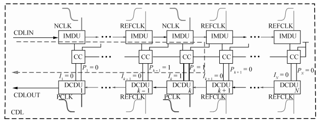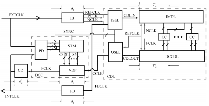
Fig. 1.
Diagram of the HPSC.
SEMICONDUCTOR INTEGRATED CIRCUITS
Chong Lu1, 2, Hongzhou Tan1, 2, Zhikui Duan2 and Yi Ding2
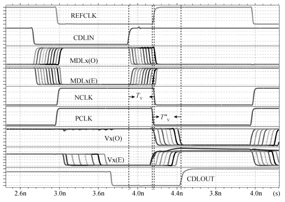
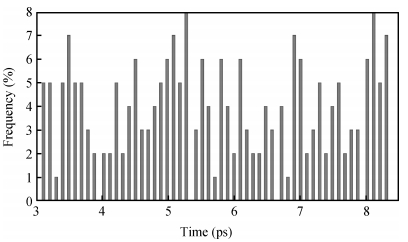
Abstract: In this paper, a novel structure of a high-precision synchronization circuit, HPSC, using interleaved delay units and a dynamic compensation circuit is proposed.HPSCs are designed for synchronization of clock distribution networks in large-scale integrated circuits, where high-quality clocks are required.The application of a hybrid structure of a coarse delay line and dynamic compensation circuit performs roughly the alignment of the clock signal in two clock cycles, and finishes the fine tuning in the next three clock cycles with the phase error suppressed under 3.8 ps.The proposed circuit is implemented and fabricated using a SMIC 0.13 μm 1P6M process with a supply voltage at 1.2 V.The allowed operation frequency ranges from 200 to 800 MHz, and the duty cycle ranges between [20%,80%].The active area of the core circuits is 245×134 μm2, and the power consumption is 1.64 mW at 500 MHz.
Keywords: HPSC, clock synchronization circuit, SMD, dynamic compensation circuit, binary search, interleaved delay units
| [1] | |
| [2] | |
| [3] | |
| [4] | |
| [5] | |
| [6] | |
| [7] | |
| [8] | |
| [9] | |
| [10] | |
| [11] | |
| [12] | |
| [13] | |
| [14] | |
| [15] | |
| [16] | |
| [17] | |
| [18] | |
| [19] | |
| [20] | |
| [21] | |
| [22] | |
| [23] | |
| [24] |
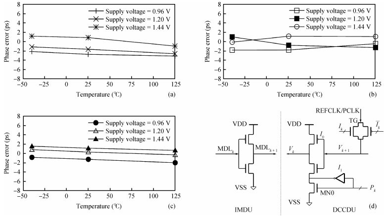
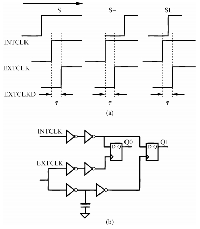
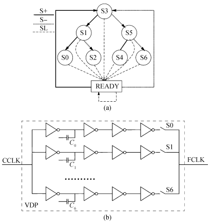
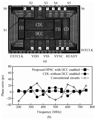
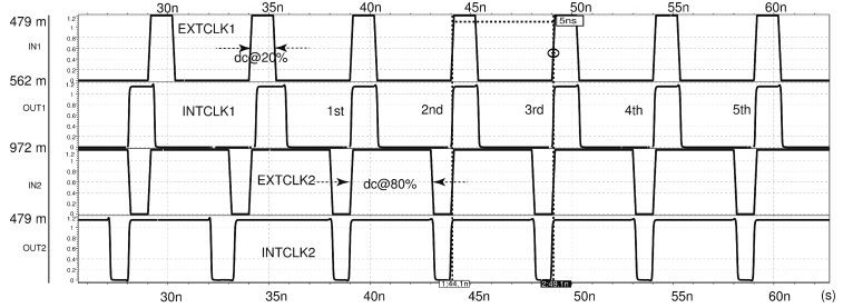
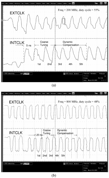
Table 1. Comparisons with other synchronization circuits.
| Parameter | JSSC04$^{[19]}$ | ISCAS05$^{[20]}$ | VLSI12$^{[24]}$ | APCCAS12$^{[23]}$ | CICC13$^{[16]}$ | This work |
| Process (nm) | 350 | 180 | 130 | 180 | 130 | 130 |
| Supply Voltage (V) | 3.3 | 1.8 | 1.2 | 1.8 | 1.5 | 1.2 |
| Frequency (MHz) | 170-230 | 200-400 | 300-800 | 150-900 | 80-450 | 200-800 |
| Area (mm$^2$) | 0.79 | -- | 0.015 | -- | -- | 0.03 |
| Power (mW) | 14.85 @ 230~MHz | 9.87 @ 400 MHz | 2.4 @ 800 MHz | 15 | 26 | 1.6 @ 500 MHz |
| Jitter[rms] (ps) | 9.9 @ 230 MHz | -- | 2.25 @ 800 MHz | -- | 2.3 @ 180 MHz | 2.2 @ 500 MHz |
| Jitter[p2p] | 72.7 @ 230 MHz | -- | 21.53 @ 800 MHz | -- | 10 @ 180 MHz | 20.8 @ 500 MHz |
| Alignment Period (cycles) | 10 | 2 | 6 | 6 | 8 | 5 |
| Phase error (ps) | 140 | 58.7 | 31.2 | 45 | 15 | 3.8 |
 DownLoad: CSV
| [1] | |
| [2] | |
| [3] | |
| [4] | |
| [5] | |
| [6] | |
| [7] | |
| [8] | |
| [9] | |
| [10] | |
| [11] | |
| [12] | |
| [13] | |
| [14] | |
| [15] | |
| [16] | |
| [17] | |
| [18] | |
| [19] | |
| [20] | |
| [21] | |
| [22] | |
| [23] | |
| [24] |


Article views: 2934 Times PDF downloads: 17 Times Cited by: 0 Times
Received: 07 April 2015 Revised: Online: Published: 01 October 2015
| Citation: |
Chong Lu, Hongzhou Tan, Zhikui Duan, Yi Ding. A high-precision synchronization circuit for clock distribution[J]. Journal of Semiconductors, 2015, 36(10): 105004. doi: 10.1088/1674-4926/36/10/105004
****
C Lu, H Z Tan, Z K Duan, Y Ding. A high-precision synchronization circuit for clock distribution[J]. J. Semicond., 2015, 36(10): 105004. doi: 10.1088/1674-4926/36/10/105004.

|
| [1] | |
| [2] | |
| [3] | |
| [4] | |
| [5] | |
| [6] | |
| [7] | |
| [8] | |
| [9] | |
| [10] | |
| [11] | |
| [12] | |
| [13] | |
| [14] | |
| [15] | |
| [16] | |
| [17] | |
| [18] | |
| [19] | |
| [20] | |
| [21] | |
| [22] | |
| [23] | |
| [24] |

 WeChat ID
Journal of Semiconductors © 2017 All Rights Reserved 京ICP备05085259号-2