


Fig. 1.
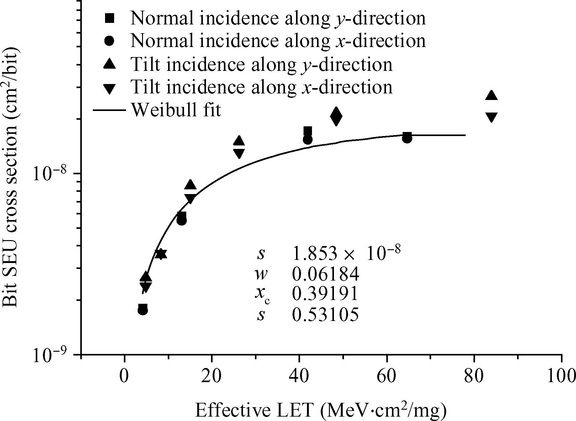
M328C heavy ion single event bit upset cross section as a function of the effective LET.
SEMICONDUCTOR DEVICES
Yinhong Luo, Fengqi Zhang, Hongxia Guo, Yao Xiao, Wen Zhao, Lili Ding and Yuanming Wang
Corresponding author: Luo Yinhong, Email: luoyinhong@nint.ac.cn
Abstract: Single event multiple-cell upsets (MCU) increase sharply with the semiconductor devices scaling. The impacts of several test factors on heavy ion single event MCU in 65 nm SRAM are studied based on the buildup of MCU test data acquiring and processing technique, including the heavy ion LET, the tilt angle, the device orientation, the test pattern and the supply voltage; the MCU physical bitmaps are extracted correspondingly. The dependencies of parameters such as the MCU percentage, MCU mean and topological pattern on these factors are summarized and analyzed. This work is meaningful for developing a more reasonable single event test method and assessing the effectiveness of anti-MCU strategies on nanometer-scale devices.
Keywords: multiple-cell upsets, nanometer-scale SRAM, test factors, device orientation
| [1] | |
| [2] | |
| [3] | |
| [4] | |
| [5] | |
| [6] | |
| [7] |

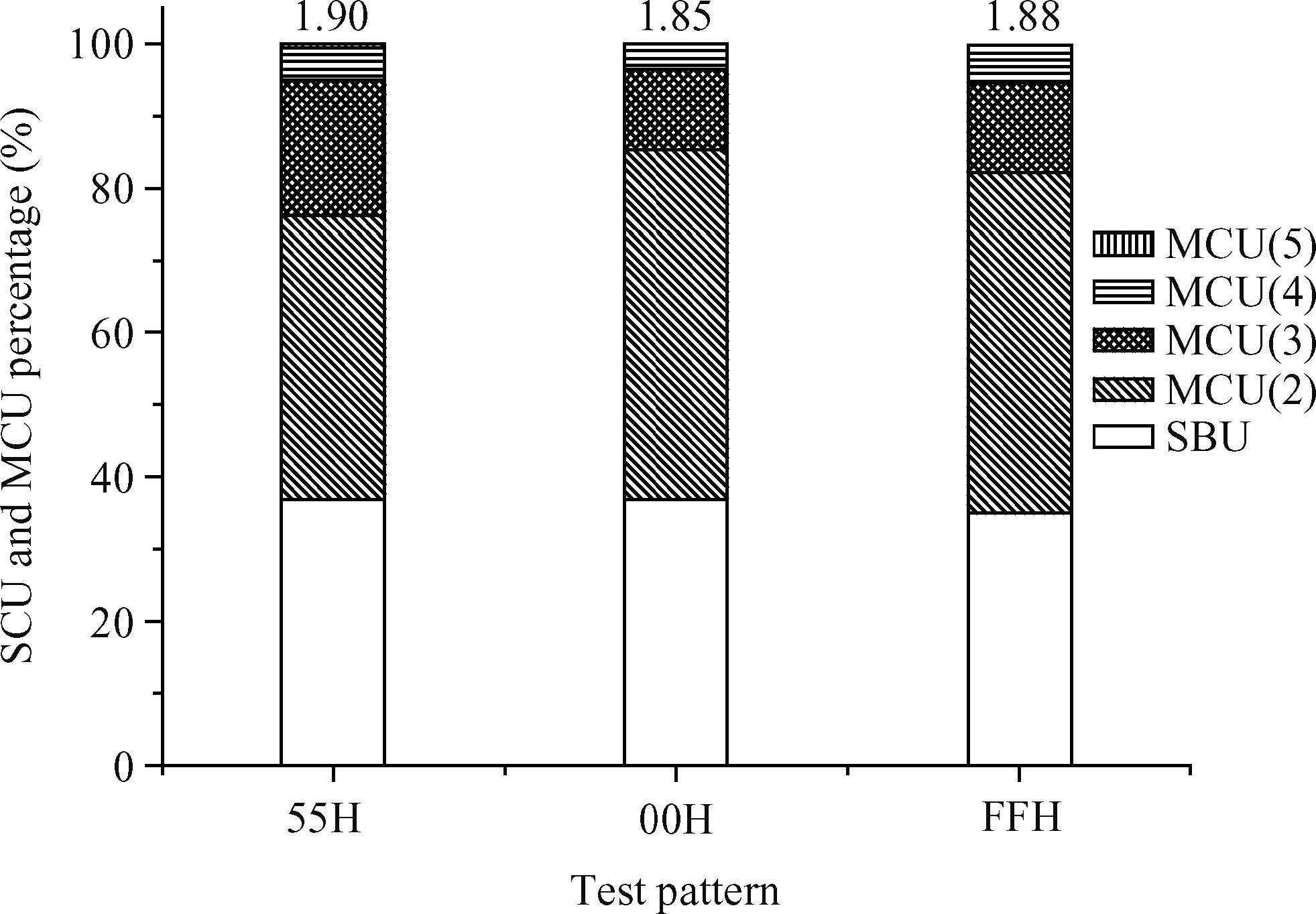
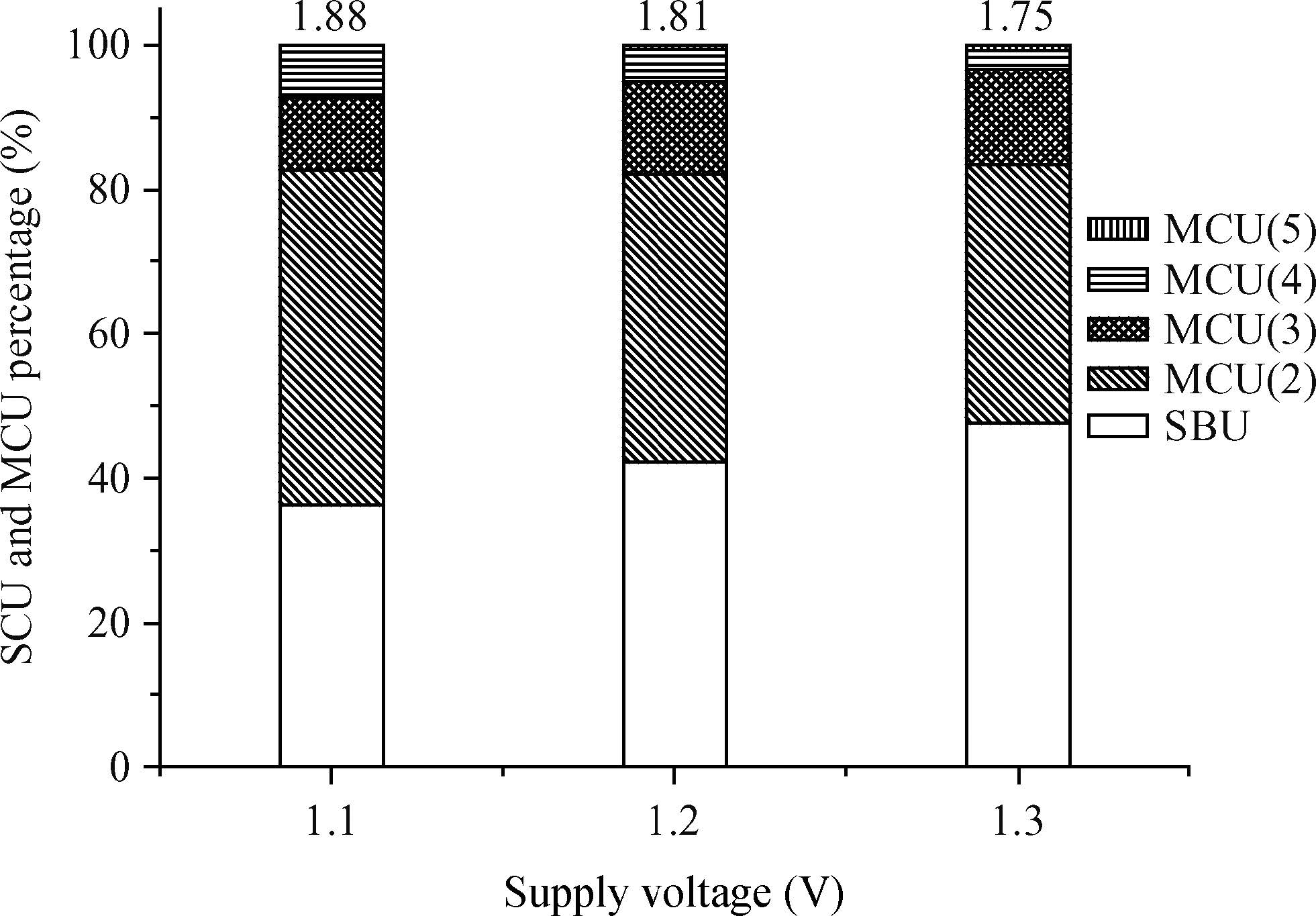
Table 3. MCU percentage of different topological pattern versus device orientation for fluorine ion.
 DownLoad: CSV
| [1] | |
| [2] | |
| [3] | |
| [4] | |
| [5] | |
| [6] | |
| [7] |


Article views: 3329 Times PDF downloads: 12 Times Cited by: 0 Times
Received: 11 June 2015 Revised: Online: Published: 01 November 2015
| Citation: |
Yinhong Luo, Fengqi Zhang, Hongxia Guo, Yao Xiao, Wen Zhao, Lili Ding, Yuanming Wang. Impacts of test factors on heavy ion single event multiple-cell upsets in nanometer-scale SRAM[J]. Journal of Semiconductors, 2015, 36(11): 114009. doi: 10.1088/1674-4926/36/11/114009
****
Y H Luo, F Q Zhang, H X Guo, Y Xiao, W Zhao, L L Ding, Y M Wang. Impacts of test factors on heavy ion single event multiple-cell upsets in nanometer-scale SRAM[J]. J. Semicond., 2015, 36(11): 114009. doi: 10.1088/1674-4926/36/11/114009.

|
| [1] | |
| [2] | |
| [3] | |
| [4] | |
| [5] | |
| [6] | |
| [7] |

 WeChat ID
Journal of Semiconductors © 2017 All Rights Reserved 京ICP备05085259号-2


