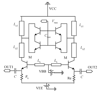
Fig. 1.
Diagram of single-ended VCO with CE configuration and $\pi $-networks.
SEMICONDUCTOR INTEGRATED CIRCUITS
Ting Yan, Yuming Zhang, Hongliang Lü, Yimen Zhang, Yue Wu and Yifeng Liu
Corresponding author: Hongliang Lü, E-mail: hllv@mail.xidian.edu.cn
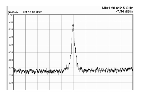
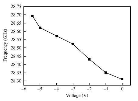
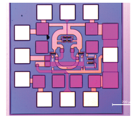
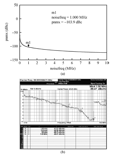
Abstract: Design and fabrication of a Ka-band voltage-controlled oscillator (VCO) using commercially available 1-μm GaAs heterojunction bipolar transistor technology is presented. A fully differential common-emitter configuration with a symmetric capacitance with a symmetric inductance tank structure is employed to reduce the phase noise of the VCO, and a novel π-feedback network is applied to compensate for the 180° phase shift. The on-wafer test shows that the VCO exhibits a phase noise of —96.47 dBc/Hz at a 1 MHz offset and presents a tuning range from 28.312 to 28.695 GHz. The overall dc current consumption of the VCO is 18 mA with a supply voltage of -6 V. The chip area of the VCO is 0.7 × 0.7 mm2.
Keywords: VCO, GaAs HBT, common-emitter, phase noise, π -feedback
| [1] | |
| [2] | |
| [3] | |
| [4] | |
| [5] | |
| [6] | |
| [7] | |
| [8] | |
| [9] | |
| [10] | |
| [11] | |
| [12] | |
| [13] | |
| [14] |
| [1] | |
| [2] | |
| [3] | |
| [4] | |
| [5] | |
| [6] | |
| [7] | |
| [8] | |
| [9] | |
| [10] | |
| [11] | |
| [12] | |
| [13] | |
| [14] |


Article views: 3464 Times PDF downloads: 33 Times Cited by: 0 Times
Received: 03 July 2014 Revised: Online: Published: 01 February 2015
| Citation: |
Ting Yan, Yuming Zhang, Hongliang Lü, Yimen Zhang, Yue Wu, Yifeng Liu. Low phase noise GaAs HBT VCO in Ka-band[J]. Journal of Semiconductors, 2015, 36(2): 025001. doi: 10.1088/1674-4926/36/2/025001
****
T Yan, Y M Zhang, H Lü, Y M Zhang, Y Wu, Y F Liu. Low phase noise GaAs HBT VCO in Ka-band[J]. J. Semicond., 2015, 36(2): 025001. doi: 10.1088/1674-4926/36/2/025001.

|
| [1] | |
| [2] | |
| [3] | |
| [4] | |
| [5] | |
| [6] | |
| [7] | |
| [8] | |
| [9] | |
| [10] | |
| [11] | |
| [12] | |
| [13] | |
| [14] |

 WeChat ID
Journal of Semiconductors © 2017 All Rights Reserved 京ICP备05085259号-2

 DownLoad: