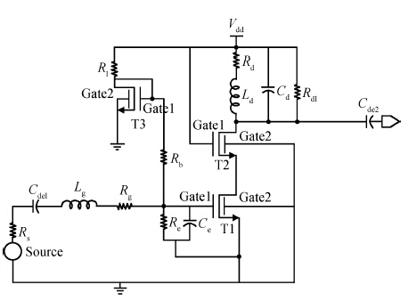
Fig. 1.
The LNA circuit considered in this study.
SEMICONDUCTOR INTEGRATED CIRCUITS
D. Suresh1, K. K. Nagarajan2 and R. Srinivasan3
Corresponding author: D. Suresh, E-mail: dsureshh89@gmail.com
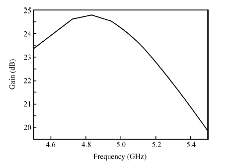
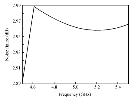
Abstract: The effect of process variations of a FinFET-based low noise amplifier (LNA) are mitigated by using the device in an independently driven mode, i.e. an independently driven double gate (IDDG) FinFET. A 45 nm gate length IDDG FinFET-based cascoded LNA, operating at 5 GHz, is designed and studied to assess the impact of process variation on the LNA performance metrics such as input impedance, gain and noise figure. Four geometrical parameters, gate length, channel width, gate oxide thickness and fin width, and one non-geometrical parameter, channel doping concentration, are considered in the study. The effect of these variations on the input impedance (the desired value is 50 Ω purely real) of the LNA is compensated by the second gate bias of the IDDG FinFET.
Keywords: FinFET, LNA, process variation, T-SPICE
| [1] | |
| [2] | |
| [3] | |
| [4] | |
| [5] | |
| [6] | |
| [7] | |
| [8] | |
| [9] | |
| [10] | |
| [11] | |
| [12] |
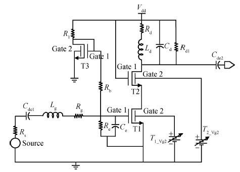
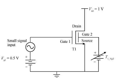
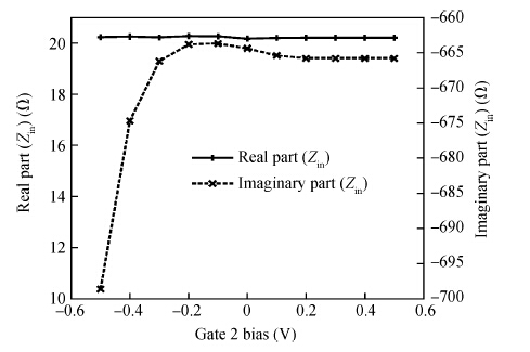
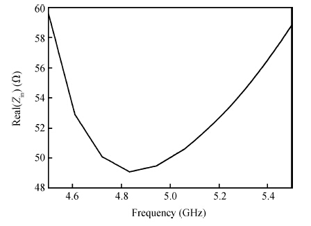
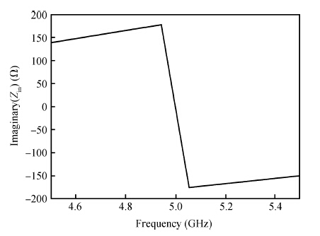
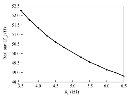
Table 7. The effect of process variation on Re[$Z_{\rm in}$] and Im[$Z_{\rm in}$] and its compensation.
 DownLoad: CSV
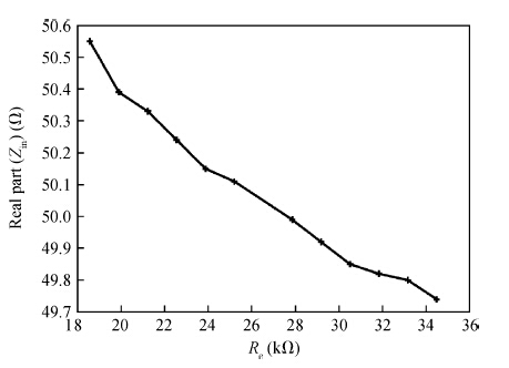
Table 8. The impact of $R_{\rm B}$ and $R_{\rm e}$ on the input impedance before and after matching.
DownLoad: CSV
| [1] | |
| [2] | |
| [3] | |
| [4] | |
| [5] | |
| [6] | |
| [7] | |
| [8] | |
| [9] | |
| [10] | |
| [11] | |
| [12] |


Article views: 3601 Times PDF downloads: 33 Times Cited by: 0 Times
Received: 09 September 2014 Revised: Online: Published: 01 April 2015
| Citation: |
D. Suresh, K. K. Nagarajan, R. Srinivasan. The impact of process variations on input impedance and mitigation using a circuit technique in FinFET-based LNA[J]. Journal of Semiconductors, 2015, 36(4): 045002. doi: 10.1088/1674-4926/36/4/045002
****
D. Suresh, K. K. Nagarajan, R. Srinivasan. The impact of process variations on input impedance and mitigation using a circuit technique in FinFET-based LNA[J]. J. Semicond., 2015, 36(4): 045002. doi: 10.1088/1674-4926/36/4/045002.

|
| [1] | |
| [2] | |
| [3] | |
| [4] | |
| [5] | |
| [6] | |
| [7] | |
| [8] | |
| [9] | |
| [10] | |
| [11] | |
| [12] |

 WeChat ID
Journal of Semiconductors © 2017 All Rights Reserved 京ICP备05085259号-2