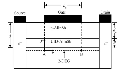
Loading [MathJax]/jax/output/HTML-CSS/jax.js
J. Semicond. > 2015, Volume 36 > Issue 6 > 064003

SEMICONDUCTOR DEVICES

Analysis of charge density and Fermi level of AlInSb/InSb single-gate high electron mobility transistor

S. Theodore Chandra1, N. B. Balamurugan1, M. Bhuvaneswari2, N. Anbuselvan2 and N. Mohankumar2

+ Author Affiliations

 Corresponding author: E-amil: theodore@tce.edu

DOI: 10.1088/1674-4926/36/6/064003

PDF

Abstract: A compact model is proposed to derive the charge density of the AlInSb/InSb HEMT devices by considering the variation of Fermi level, the first subband, the second subband and sheet carrier charge density with applied gate voltage. The proposed model considers the Fermi level dependence of charge density and vice versa. The analytical results generated by the proposed model are compared and they agree well with the experimental results. The developed model can be used to implement a physics based compact model for an InSb HEMT device in SPICE applications.

Key words: charge densityFermi levelhigh electron mobility transistor2D analytical model

Indium antimonide has the highest electron mobility and saturation velocity of any known semiconductor, and is therefore a promising material for ultra-high-speed devices[1, 2]. InSb quantum-well (QW) transistors formed by AlInSb/InSb heterostructure have been under the spotlight recently due to their remarkable potential in low power/voltage and high-speed circuits[3]. It has been observed that to achieve the same performance as the state-of-the-art silicon MOSFETs, InSb QW-FETs consume about 10% in power owing to extremely high electron mobility (as high as 30000 cm2/(Vs)) and saturation velocity (5.107 cm/s) in the channel region of the III-V semiconductors, InSb has the lightest effective mass and narrowest band gap along with a large dielectric constant (ε) and an exceptionally large Lande g-factor of 51 in bulk and as large as 60 in quantum well heterostructures[4]. These properties make it an exciting candidate for many different applications including high speed electronics and spintronics. Hence InSb heterostructure is chosen for high speed electronics, where significant advancements have been made in both n- and p-channel field effect transistors (FET) for digital and analogue applications, quantum and spintronics applications where the large g-factor may give rise to all electron spin manipulation and ballistic transport devices where the large ballistic length may give rise to ultra sensitive magnetic field sensors[5]. These have been widely investigated in III-V semiconductors such as GaAs, but development in InSb-based systems is not so far progressed. AlInSb/InSb high electron mobility transistor (HEMT) devices are considered to be very promising candidates for high-speed and high-power applications[6]. These devices offer an advantage such as high breakdown voltage, high charge density and good electron mobility. The formation of the 2-D electron gas (2DEG) in these devices is the heart during the device operation. For accurate and fast simulation of circuits based on these devices, an analytical expression for 2DEG density ns is required. The expression should be also physics based, which obviates the use of a large number of empirical parameters. The currently available models for charge density are primarily based on numerical calculations, semi empirical model expressions, or simplifying approximations[7, 8, 9]. Models relying on numeric calculations will be slow because of the iterative nature. Semi empirical models are fast but do not provide the necessary insight into the device operation. They also tend to have a large number of empirical parameters, which have to be extracted from experimental data[10, 11]. In contrast to these approaches, we have obtained an accurate physics-based analytical model for charge density and Fermi level in the AlInSb/InSb HEMT device with minimal empirical parameters in this paper. For this purpose, the sheet charge density equation of the 2DEG region is used and it is assumed that the AlInSb layer is completely ionized in the device.

The rest of the paper is organized as follows: Section 2 presents the schematic device structure of the AlInSb/InSb HEMT device. Section 3 deals with the model formulation of charge density and Fermi level for the AlInSb/InSb HEMT device. Also, the unified charge density model for the AlInSb/InSb HEMT device is discussed in Section 4. Results and the discussions are presented in Section 5. The conclusion is given in Section 6.

The cross-sectional view of the AlInSb/InSb HEMT device for two different experimentally determined positions of the 2DEG channel in the device structure is shown in Figure 1. The layer sequence, from bottom to top, is InSb-undoped/UID-AlInSb/n-AlInSb/metal, with 2DEG channel formed in the interface between InSb-undoped/UID-AlInSb.

Figure  1.  Cross-sectional view of AlInSb/InSb HEMTs with gate length Lg, di spacer layer thickness and dd n-AlInSb layer thickness.

A doped AlInSb barrier layer saves the carriers from Coulomb scattering caused by ionized impurities and provides carriers a channel at a zero gate voltage. The device thus works in a depletion mode with carriers confined in the InSb quantum well. The device structure is also known as a modulation doped field-effective transistor (MODFET)[12, 13]. The quantum well formed of a ternary compound with mole fraction of Al0.3In0.7Sb/InSb HEMT is used. It has been demonstrated that when the mole fraction of Al increases to 30%, the electron wave function is perfectly confined within the well. Figure 2 shows the sub bands energy levels E1, E0 along with the conduction band in the 2DEG quantum well.

Figure  2.  Conduction band structure with sub bands and Fermi level energy levels.

The difficulty in modeling the 2DEG charge density arises from the complicated variation of Ef with ns in the quantum well[14]. This relationship is given by

ns=DVth[ln(expEfE0Vth+1)+ln(expEfE1Vth+1)], (1)
where E0=γ0n2/3s and E1=γ1n2/3s are the levels of the two lowest subbands, Ef is the Fermi level expressed in volts, and Vth=kT/q is the thermal voltage.

ns=DVth[ln(expEfE0Vth+1)]. (2)

Assuming that the AlInSb layer is completely ionized, we can write

ns=εqd(vg0Ef), (3)
where vgo=vgvoff, and voff are the cutoff voltage. The variation of ns with respect to vg is a complicated transcendental function. Hence, we propose a few assumptions in order to simplify these equations, which allow us to develop a precise analytical expression for ns versus vg for the typical operating range of gate voltages and temperatures and drain current of the AIInSb/InSb device.

Figure 3 shows important quantities Ef, E0 and E1 as obtained from numerical calculations based on Equations (1) and (2) for a wide range of gate voltages from close to voff and above. It is interesting to note the relative positions of the sub band levels when compared with Ef in this range. The charge density increases linearly with the energy bands. Upper-level E1 is larger than Ef for the complete range of gate voltages. Hence contribution to the charge density from the second sub band can be safely ignored. Here E0 have two distinct regions namely region I and region II. In region I, E0 is larger than Ef corresponding to Vgo < 0.9 V. In region II, E0 is lower than Ef corresponding to Vgo > 0.9 V. We consider the full-scale range of gate voltages except very close to cutoff. The Fermi level equation is derived as follows for the regions I and II.

Figure  3.  Numerical calculations of Ef, E0 and E1 versus gate voltage at T = 298 K.

The second term can be ignored in Equation (2) for the calculation of Fermi's level[14]. This is written in a simplified form as,

nsDVth=eEfE0vth. (4)

Taking ln on both sides

lnnsDVth=EfE0vth. (5)

By solving we get the equation for Fermi's level as follows,

Ef=γ0n2/3s+vthlnnsDVth. (6)

By considering the full-scale range of gate voltages, except very close to cutoff, Ef will be much smaller than vgo. The model for ns is separately developed in regions I and II. These models are then combined to give a unified model covering both regions.

The Fermi level in region I is given by

EIf=γ0n2/3s+vthlnnsDVth. (7)

It is important to point out here that, for vertically scaled devices with d < 5 nm, the 2DEG distance from the interface, i.e., δd, will become comparable with d. In such cases, d should be replaced by deff=d+δd in the model expressions.

The Fermi level formulation for region I is obtained by substituting the charge density equation ns to the general Fermi level equation as follows,

γ0[εqd(vgoEf)]2/3+vthln[εDvthqd(vgoEf)]=EIf. (8)

Also substituting for Cg=ε/d, and β = Cg/qDVth and solving we get Fermi's level in region I as,

EIf=vgoγ0(cgvgoq)2/3+vthlnβvgovgo+vth+23γ0(cgvgoq)2/3. (9)

Using Fermi level in region I we can derive the sheet carrier density equation in region I. Assuming that the AlInSb layer is completely ionized, we can write,

ns=εqd(vgoEf). (10)

Substituting Fermi level in region I in the above equation

ns=εqd[vgovgoγ0(cgvgoq)2/3+vthlnβvgovgo+vth+23γ0(cgvgo/q)2/3], (11)
ns=εvgoqd[1γ0(cgvgoq)2/3+vthlnβvgovgo+vth+23γ0(cgvgoq)2/3], (12)
ns=cgvgoq[1γ0(cgvgoq)2/3+vthlnβvgovgo+vth+23γ0(cgvgo/q)2/3]. (13)

We develop an analytical model for ns versus gate voltage in region I, the sheet carrier density in region I is given by,

nIs=cgvgoq[vgo+vth(1lnβvgo)γ03(cgvgoq)2/3]vgo+vth+2γ03(cgvgoq)2/3. (14)

The relationship approximate expression for nIIs and it is given by,

nIIsD(EIIfE0), (15)
nIIsD=EIIfE0, (16)
nIIsD+E0=EIIf. (17)

Since the AlInSb layer is completely ionized, we can substitute ns in the above equation.

The Fermi level formulation for region II is obtained by substituting the charge density equation to the general Fermi level.

1D[εqd(Vg0Ef)]+γ0n2/3s=EIIf, (18)
cgqD[(vgoEf)]+γ0[εqd(Vg0Ef)]23=EIIf, (19)

By solving the above equation, we get the Fermi level in region II.

EIIf=vgoβvgovth+γ03(cgvgoq)2/3vgo(1+βvth)+23γ0(cgvgoq)2/3. (20)

Since the AlInSb layer is completely ionized, we can use ns equation for substitution of Fermi level in region II. Substituting Fermi's level Ef of region II in Equation (10),

ns=εqd[vgovgoβvgovth+γ03(cgvgoq)2/3vgo(1+βvth)+23γ0(cgvgoq)2/3], (21)
ns=εvgoqd[1βvgovth+γ03(cgvgoq)2/3vgo(1+βvth)+23γ0(cgvgoq)2/3]. (22)

The sheet carrier density in region II is given by

nIIs=cgvgoqvgoγ03(cgvgoq)2/3vgo(1+βvth)+23γ0(cgvgoq)2/3. (23)

In order to find a unifying expression for Ef and ns applicable for the full-scale range of gate voltages, we observe that the respective expressions for regions I and II differ only in one term to the numerator and one term to a denominator, both with a factor of Vth. Hence, both the regional models are expected to provide a fairly reasonable approximation for full scale within the voltage range, except near cutoff. To improve accuracy, we propose to use a unified form that combines the two regional models. Specifically the expression for ns is given by

ns=cgvgoqvgo+vth[1lnβvgoγ03(cgvgoq)2/3]vgo(1+vthvgod)+23γ0(cgvgoq)2/3, (24)
Here, Vgon and Vgod are functions of Vg given by the interpolation expression.
Vgox=VgoαxV2go+α2x, (25)
where αn=eβ and αd=1β. We observe that the unified model has the proper limitation for charge density of regions I and II. A similar unified expression can be also easily established for the Fermi level by applying the unified charge density in the fundamental charge density equation.

In this model, we have discussed the AlInSb/InSb HEMT devices with two different regions for charge density, by considering the various temperatures, Fermi level regions and validated with experimental data. The model and experimental data comparisons are done for the Al0.3In0.7Sb/InSb HEMT devices by accounting corresponding permittivity and thickness are 16ε0 and 20 nm with carrier densities of 3.28 × 10¹⁵~m2 and also considering the parameters γ0, γ1 and cutoff voltage.

Figure 3 shows the Fermi level of first sub band and second sub band with the gate voltage variation. The parameters used are given in Table 1. The charge density increases linearly with the energy bands. Upper-level E1 is larger than Ef for the complete range of gate voltages. Hence contribution to the charge density from the second sub band can be safely ignored. Here E0 have two distinct regions namely regions I and II. In region I, E0 is larger than Ef corresponding to Vgo < 0.9 V. In region II where E0 is lower than Ef corresponding to Vgo > 0.9 V. We consider the full-scale range of gate voltages except very close to cutoff. Figure 4 shows the relative positions of Fermi levels with the first sub band and second sub band with the gate voltage. The Fermi level of the first sub band will not increase with charge density, but the conduction pattern of the triangular quantum well of the second sub band will cause the charge density to increase linearly with applied gate voltage.

Figure  4.  Numerical calculations of EfE0 and EfE1 versus gate voltage at T= 298 K.
Table  1.  List of symbols and parameters used.
DownLoad: CSV  | Show Table

Figures 5 and 6 show the comparison of charge density model for region I with thermal voltage for different values of gate voltage. From this plot, we can say that, the first sub band energy level increases with respect to gate voltage, which causes the energy level less than 0.9 V in region I and greater than 0.9 V in region II.

Figure  5.  Charge density for region I with thermal voltage versus gate voltage.

The observations are shown in Figures 5 and 6 such that the charge density for electron decreases while accounting for the thermal voltage and increases by leaving the thermal voltage respectively. The model results are validated with experimental data.

Figure  6.  Charge density for region I without thermal voltage versus gate voltage.

Figures 7 and 8 show the comparison of the charge density model for region II with thermal voltage for different values of gate voltage. From this plot, we can say that, second sub band energy level decreases with respect to gate voltage, which causes the energy level greater than 0.9 V in region I and less than 0.9 V in region II. The observations are shown in Figures 6 and 7 such that the charge density for electron decreases while accounting for the thermal voltage and increases by leaving the thermal voltage respectively. The model results are validated with experimental data.

Figure  7.  Charge density for region II with thermal voltage versus gate voltage.
Figure  8.  Charge density for region II without thermal voltage versus gate voltage.

Figure 9 shows the comparison of a unified model for charge density of AlInSb/InSb with the gate voltage. It is applicable for the full-scale range of gate voltage, we observe that the respective expressions for regions I and II differ only in one term to the numerator and one term to a denominator both with a factor of thermal voltage. Hence both the regional models are expected to provide a fairly reasonable approximation for full-scale voltage range, except near cutoff. For achieving accuracy, we relate the unified two regional models expression. Here the function of gate voltage is to conduct electron for on and off states. Electrons in region I perform quite well with respect to region II, electrons in region II models performs relatively poorly in region I, with a rapid increase in full-scale gate voltage.

Figure  9.  Unified model for charge density versus gate voltage.

Figure 10 shows the comparison of charge density with different temperature versus the gate voltage (T= 200, 300, 400, 500 K). From the graph, we conclude that the InSb operates at high power at elevated temperatures. In Figure 9, the unified model for charge density is compared with experiment data for different temperatures up to 500 K. It is apparent from the results that the model agrees quite well with the experimental data throughout the temperature range. The increase in error is found to be almost linear with increasing temperature for bias point gate voltage is 0.2 V.

Figure  10.  Charge density at various temperatures (T= 200, 300, 400, 500 K) versus gate voltage.

In this work, a compact model has been derived for the AlInSb/InSb devices and to vary the structural parameters of the device by considering the variation of Fermi level (Ef), the first subband E0, the second subband E1 and sheet carrier charge density (ns) with applied gate voltage (Vg) and compare the performance from the device with various temperatures. The results generated by this model agree with the experimental results.


[1]
[2]
[3]
[4]
[5]
[6]
[7]
[8]
[9]
[10]
[11]
[12]
[13]
[14]
Fig. 1.  Cross-sectional view of AlInSb/InSb HEMTs with gate length Lg, di spacer layer thickness and dd n-AlInSb layer thickness.

Fig. 2.  Conduction band structure with sub bands and Fermi level energy levels.

Fig. 3.  Numerical calculations of Ef, E0 and E1 versus gate voltage at T = 298 K.

Fig. 4.  Numerical calculations of EfE0 and EfE1 versus gate voltage at T= 298 K.

Fig. 5.  Charge density for region I with thermal voltage versus gate voltage.

Fig. 6.  Charge density for region I without thermal voltage versus gate voltage.

Fig. 7.  Charge density for region II with thermal voltage versus gate voltage.

Fig. 8.  Charge density for region II without thermal voltage versus gate voltage.

Fig. 9.  Unified model for charge density versus gate voltage.

Fig. 10.  Charge density at various temperatures (T= 200, 300, 400, 500 K) versus gate voltage.

DownLoad: CSV
DownLoad: CSV
DownLoad: CSV
DownLoad: CSV

Table 1.   List of symbols and parameters used.

DownLoad: CSV
[1]
[2]
[3]
[4]
[5]
[6]
[7]
[8]
[9]
[10]
[11]
[12]
[13]
[14]
1

Modeling on oxide dependent 2DEG sheet charge density and threshold voltage in AlGaN/GaN MOSHEMT

J. Panda, K. Jena, R. Swain, T. R. Lenka

Journal of Semiconductors, 2016, 37(4): 044003. doi: 10.1088/1674-4926/37/4/044003

2

Detection of lead ions with AlGaAs/InGaAs pseudomorphic high electron mobility transistor

Jiqiang Niu, Yang Zhang, Min Guan, Chengyan Wang, Lijie Cui, et al.

Journal of Semiconductors, 2016, 37(11): 114003. doi: 10.1088/1674-4926/37/11/114003

3

Semiconductor steady state defect effective Fermi level and deep level transient spectroscopy depth profiling

Ken K. Chin, Zimeng Cheng

Journal of Semiconductors, 2016, 37(9): 092003. doi: 10.1088/1674-4926/37/9/092003

4

Effects of interface trap density on the electrical performance of amorphous InSnZnO thin-film transistor

Yongye Liang, Kyungsoo Jang, S. Velumani, Cam Phu Thi Nguyen, Junsin Yi, et al.

Journal of Semiconductors, 2015, 36(2): 024007. doi: 10.1088/1674-4926/36/2/024007

5

Insights into channel potentials and electron quasi-Fermi potentials for DGtunnel FETs

Menka, Anand Bulusu, S. Dasgupta

Journal of Semiconductors, 2015, 36(1): 014005. doi: 10.1088/1674-4926/36/1/014005

6

Analytical modeling and simulation of germanium single gate silicon on insulator TFET

T. S. Arun Samuel, N. B. Balamurugan

Journal of Semiconductors, 2014, 35(3): 034002. doi: 10.1088/1674-4926/35/3/034002

7

Model development for analyzing 2DEG sheet charge density and threshold voltage considering interface DOS for AlInN/GaN MOSHEMT

Devashish Pandey, T.R. Lenka

Journal of Semiconductors, 2014, 35(10): 104001. doi: 10.1088/1674-4926/35/10/104001

8

Compact analytical model for single gate AlInSb/InSb high electron mobility transistors

S. Theodore Chandra, N.B. Balamurugan, G. Subalakshmi, T. Shalini, G. Lakshmi Priya, et al.

Journal of Semiconductors, 2014, 35(11): 114003. doi: 10.1088/1674-4926/35/11/114003

9

Modeling and simulation of centroid and inversion charge density in cylindrical surrounding gate MOSFETs including quantum effects

P. Vimala, N. B. Balamurugan

Journal of Semiconductors, 2013, 34(11): 114001. doi: 10.1088/1674-4926/34/11/114001

10

A 2DEG charge density based drain current model for various Al and In molefraction mobility dependent nano-scale AlInGaN/AlN/GaN HEMT devices

Godwin Raj, Hemant Pardeshi, Sudhansu Kumar Pati, N Mohankumar, Chandan Kumar Sarkar, et al.

Journal of Semiconductors, 2013, 34(4): 044002. doi: 10.1088/1674-4926/34/4/044002

11

Approximate Graphic Method for Solving Fermi Level and Majority Carrier Density of Semiconductors with Multiple Donors and Multiple Acceptors

Ken K. Chin

Journal of Semiconductors, 2011, 32(6): 062001. doi: 10.1088/1674-4926/32/6/062001

12

SPICE compatible analytical electron mobility model for biaxial strained-Si-MOSFETs

Amit Chaudhry, J. N. Roy, S. Sangwan

Journal of Semiconductors, 2011, 32(5): 054001. doi: 10.1088/1674-4926/32/5/054001

13

Local charge neutrality condition, Fermi level and majority carrier density of a semiconductor with multiple localized multi-level intrinsic/impurity defects

Ken K. Chin

Journal of Semiconductors, 2011, 32(11): 112001. doi: 10.1088/1674-4926/32/11/112001

14

Monolithic Integration of Resonant Tunneling Diodes and High Electron Mobility Transistors on InP Substrates

Ma Long, Zhang Yang, Dai Yang, Yang Fuhua, Zeng Yiping, et al.

Chinese Journal of Semiconductors , 2007, 28(S1): 414-417.

15

2D Threshold-Voltage Model for High-k Gate-Dielectric MOSFETs

Ji Feng, Xu Jingping, Lai P T, Chen Weibing, Li Yanping, et al.

Chinese Journal of Semiconductors , 2006, 27(10): 1725-1731.

16

An Analytical Model for the Surface Electrical Field Distribution and Optimization of Bulk-Silicon Double RESURF Devices

Li Qi, Li Zhaoji, Zhang Bo

Chinese Journal of Semiconductors , 2006, 27(7): 1177-1182.

17

Study of Electron Mobility in 4H-SiC Buried-Channel MOSFETs

Gao Jinxia, Zhang Yimen, Zhang Yuming

Chinese Journal of Semiconductors , 2006, 27(2): 283-289.

18

Average-Bond-Energy and Fermi Level on Metal-Semiconductor Contacts

Li Shuping, Wang Renzhi

Chinese Journal of Semiconductors , 2006, 27(5): 834-839.

19

Neural-Network-Based Charge Density Quantum Correction of Nanoscale MOSFETs

Li Zunchao, Jiang Yaolin, Zhang Ruizhi

Chinese Journal of Semiconductors , 2006, 27(3): 438-442.

20

AlGaN/GaN High Electron Mobility Transistors on Sapphires with fmax of 100GHz

Li Xianjie, Zeng Qingming, Zhou Zhou, Liu Yugui, Qiao Shuyun, et al.

Chinese Journal of Semiconductors , 2005, 26(11): 2049-2052.

1. Anbuselvan, N., Anandan, P. ANN based AlGaN HEMTs Small Signal Extraction Parameter Techniques for High Power Application Devices. 2024. doi:10.1109/ICEES61253.2024.10776942
2. Anbuselvan, N., Anandan, P. Analyzing Measured and De-Embedded S-Parameters of a Hybrid Network Unit for RF Characteristics of AlGaN HEMTs. 2024. doi:10.1109/APCI61480.2024.10616797
3. Rouag, N., Trad, M., Aounallah, B. et al. Analytic solution of carrier concentration as an explicit function of gate voltage in AlGaN/GaN HEMTs using the Lambert W-function. International Journal of Numerical Modelling: Electronic Networks, Devices and Fields, 2023, 36(6): e3115. doi:10.1002/jnm.3115
4. Anbuselvan, N., Mohankumar, N., Mohanbabu, A. Analytical modeling of 2DEG with 2DHG polarization charge density drain current and small-signal model of quaternary AlInGaN HEMTs for microwave frequency applications. International Journal of Numerical Modelling: Electronic Networks, Devices and Fields, 2019, 32(5): e2609. doi:10.1002/jnm.2609
5. Chin, K.K., Cheng, Z. Semiconductor steady state defect effective Fermi level and deep level transient spectroscopy depth profiling. Journal of Semiconductors, 2016, 37(9): 092003. doi:10.1088/1674-4926/37/9/092003
  • Search

    Advanced Search >>

    GET CITATION

    Chaoqun Xu, Ying Sun, Yan Han, Dazhong Zhu. Double junction photodiode for X-ray CMOS sensor IC[J]. Journal of Semiconductors, 2014, 35(7): 074011. doi: 10.1088/1674-4926/35/7/074011
    C Q Xu, Y Sun, Y Han, D Z Zhu. Double junction photodiode for X-ray CMOS sensor IC[J]. J. Semicond., 2014, 35(7): 074011. doi: 10.1088/1674-4926/35/7/074011.
    shu

    Export: BibTex EndNote

    Article Metrics

    Article views: 2944 Times PDF downloads: 30 Times Cited by: 5 Times

    History

    Received: 13 December 2014 Revised: Online: Published: 01 June 2015

    Catalog

      Email This Article

      User name:
      Email:*请输入正确邮箱
      Code:*验证码错误
      S. Theodore Chandra, N. B. Balamurugan, M. Bhuvaneswari, N. Anbuselvan, N. Mohankumar. Analysis of charge density and Fermi level of AlInSb/InSb single-gate high electron mobility transistor[J]. Journal of Semiconductors, 2015, 36(6): 064003. doi: 10.1088/1674-4926/36/6/064003 ****S. T. Chandra, N. B. Balamurugan, M. Bhuvaneswari, N. Anbuselvan, N. Mohankumar. Analysis of charge density and Fermi level of AlInSb/InSb single-gate high electron mobility transistor[J]. J. Semicond., 2015, 36(6): 064003. doi:  10.1088/1674-4926/36/6/064003.
      Citation:
      S. Theodore Chandra, N. B. Balamurugan, M. Bhuvaneswari, N. Anbuselvan, N. Mohankumar. Analysis of charge density and Fermi level of AlInSb/InSb single-gate high electron mobility transistor[J]. Journal of Semiconductors, 2015, 36(6): 064003. doi: 10.1088/1674-4926/36/6/064003 ****
      S. T. Chandra, N. B. Balamurugan, M. Bhuvaneswari, N. Anbuselvan, N. Mohankumar. Analysis of charge density and Fermi level of AlInSb/InSb single-gate high electron mobility transistor[J]. J. Semicond., 2015, 36(6): 064003. doi:  10.1088/1674-4926/36/6/064003.

      Analysis of charge density and Fermi level of AlInSb/InSb single-gate high electron mobility transistor

      DOI: 10.1088/1674-4926/36/6/064003
      Funds:

      Project supported by the Council of Scientific & Industrial Research (CSIR), India under the Senior Research Fellowship Scheme (No. 08/237(0005)/2012-EMR-I).

      More Information
      • Corresponding author: E-amil: theodore@tce.edu
      • Received Date: 2014-12-13
      • Accepted Date: 2015-01-21
      • Published Date: 2015-01-25

      Catalog

        /

        DownLoad:  Full-Size Img  PowerPoint
        Return
        Return