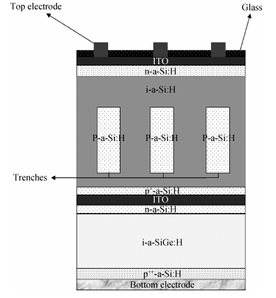
Processing math: 100%
J. Semicond. > 2015, Volume 36 > Issue 6 > 064004

SEMICONDUCTOR DEVICES

Numerical investigation of a double-junction a:SiGe thin-film solar cell including the multi-trench region

K. Kacha1, F. Djeffal1, 2, H. Ferhati1, D. Arar1 and M. Meguellati1

+ Author Affiliations

 Corresponding author: F. Djeffal, Email: djeffal@univ-batna.dz;faycaldzdz@hotmail.com

DOI: 10.1088/1674-4926/36/6/064004

PDF

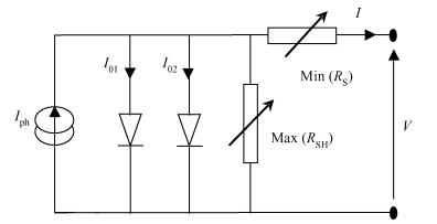
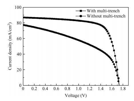
Abstract: We present a new approach based on the multi-trench technique to improve the electrical performances, which are the fill factor and the electrical efficiency. The key idea behind this approach is to introduce a new multi-trench region in the intrinsic layer, in order to modulate the total resistance of the solar cell. Based on 2-D numerical investigation and optimization of amorphous SiGe double-junction (a-Si:H/a-SiGe:H) thin film solar cells, in the present paper numerical models of electrical and optical parameters are developed to explain the impact of the multi-trench technique on the improvement of the double-junction solar cell electrical behavior for high performance photovoltaic applications. In this context, electrical characteristics of the proposed design are analyzed and compared with conventional amorphous silicon double-junction thin-film solar cells.

Key words: amorphousefficiencySiGethin-filmsolar cellmulti-trench


[1]
[2]
[3]
[4]
[5]
[6]
[7]
[8]
[9]
[10]
[11]
Fig. 1.  Cross sectional view of the investigated amorphous double-junction SiGe thin-film solar cell.

Fig. 2.  Equivalent electrical circuit of the investigated solar cell.

Fig. 3.  Variation of solar cell efficiency as function of (a) trench doping concentration,(b) trench width and (c) trench thickness.

Fig. 4.  Efficiency of the investigated solar cell as a function of the number of trenches in the frontal intrinsic layer.

Fig. 5.  Efficiency of the investigated solar cell as a function of Ge content in the back amorphous SiGe intrinsic layer (N= 3).

Fig. 6.  Solar cell performance with different back intrinsic region thickness values,Ge mole fraction = 0.5 and N= 3.

Fig. 7.  I-V curves of the optimized multi-trench and conventional solar cells (N=3).

Table 1.   Optimized design parameters used in our investigation.

DownLoad: CSV

Table 2.   Optimized solar cell performances.

DownLoad: CSV
[1]
[2]
[3]
[4]
[5]
[6]
[7]
[8]
[9]
[10]
[11]
1

Large area perovskite solar cell module

Longhua Cai, Lusheng Liang, Jifeng Wu, Bin Ding, Lili Gao, et al.

Journal of Semiconductors, 2017, 38(1): 014006. doi: 10.1088/1674-4926/38/1/014006

2

The effect of multi-intermediate bands on the behavior of an InAs1-xNx/GaAs1-ySby quantum dot solar cell

Abou El-Maaty M. Aly, A. Nasr

Journal of Semiconductors, 2015, 36(4): 042001. doi: 10.1088/1674-4926/36/4/042001

3

Effects of interface trap density on the electrical performance of amorphous InSnZnO thin-film transistor

Yongye Liang, Kyungsoo Jang, S. Velumani, Cam Phu Thi Nguyen, Junsin Yi, et al.

Journal of Semiconductors, 2015, 36(2): 024007. doi: 10.1088/1674-4926/36/2/024007

4

Dynamic threshold voltage operation in Si and SiGe source junctionless tunnel field effect transistor

Shibir Basak, Pranav Kumar Asthana, Yogesh Goswami, Bahniman Ghosh

Journal of Semiconductors, 2014, 35(11): 114001. doi: 10.1088/1674-4926/35/11/114001

5

Modified textured surface MOCVD-ZnO:B transparent conductive layers for thin-film solar cells

Xinliang Chen, Congbo Yan, Xinhua Geng, Dekun Zhang, Changchun Wei, et al.

Journal of Semiconductors, 2014, 35(4): 043002. doi: 10.1088/1674-4926/35/4/043002

6

Optical and electrical properties of porous silicon layer formed on the textured surface by electrochemical etching

Ou Weiying, Zhao Lei, Diao Hongwei, Zhang Jun, Wang Wenjing, et al.

Journal of Semiconductors, 2011, 32(5): 056002. doi: 10.1088/1674-4926/32/5/056002

7

A 2.1–6 GHz SiGe BiCMOS low-noise amplifier design for a multi-mode wideband receiver

Chen Lei, Ruan Ying, Ma Heliang, Lai Zongsheng

Journal of Semiconductors, 2010, 31(5): 055001. doi: 10.1088/1674-4926/31/5/055001

8

Theoretical investigation of efficiency of a p-a-SiC:H/i-a-Si:H/n-μc-Si solar cell

Deng Qingwen, Wang Xiaoliang, Xiao Hongling, Ma Zeyu, Zhang Xiaobin, et al.

Journal of Semiconductors, 2010, 31(10): 103003. doi: 10.1088/1674-4926/31/10/103003

9

Growth of SiGe by D-UHV/CVD at Low Temperature

Zeng Yugang, Han Genquan, Yu Jinzhong

Journal of Semiconductors, 2008, 29(10): 1889-1892.

10

Strain and Annealing Effect of SiGe/Si Heterostructure in Limited Area Grown by MBE

Yang Hongbin, Fan Yongliang, Zhang Xiangjiu

Chinese Journal of Semiconductors , 2007, 28(8): 1226-1231.

11

Multi-Finger Power SiGe HBT with Non-Uniform Finger Spacing

Jin Dongyue, Zhang Wanrong, Shen Pei, Xie Hongyun, Wang Yang, et al.

Chinese Journal of Semiconductors , 2007, 28(10): 1527-1531.

12

A Multi-Finger Si1-xGex/Si Heterojunction Bipolar Transistor for Wireless Power Amplifier Applications

Xue Chunlai, Shi Wenhua, Yao Fei, Cheng Buwen, Wang Hongjie, et al.

Chinese Journal of Semiconductors , 2007, 28(4): 496-499.

13

Two Kinds of Patterned SiGe Epitaxial Growth Technologies

Xu Yang, Wang Fei, Xu Jun, Liu Zhihong, Qian Peixin, et al.

Chinese Journal of Semiconductors , 2006, 27(S1): 389-391.

14

Growth and Shape Preservation of Self-Assembled SiGe Quantum Rings

Li Fanghua, Jiang Zuimin

Chinese Journal of Semiconductors , 2006, 27(S1): 148-150.

15

Space-Charge-Limited Current Properties of Amorphous GaN Thin Films

Zhang Zhenxing, Xie Erqing, Pan Xiaojun, Jia Lu, Han Weihua, et al.

Chinese Journal of Semiconductors , 2006, 27(S1): 113-116.

16

Influence of Oxidation on Residual Strain Relaxation of SiGe Film Grown on SOI Substrate

Jin Bo, Wang Xi, Chen Jing, Zhang Feng, Cheng Xinli, et al.

Chinese Journal of Semiconductors , 2006, 27(1): 86-90.

17

Effect of Si Intermediate Layer on High Relaxed SiGe Layer Grown Using Low Temperature Si Buffer

Yang Hongbin, Fan Yongliang

Chinese Journal of Semiconductors , 2006, 27(S1): 144-147.

18

Transport Current Model of SiGe HBT

Hu Huiyong, Zhang Heming, Dai Xianying, Xuan Rongxi, Cui Xiaoying, et al.

Chinese Journal of Semiconductors , 2006, 27(6): 1059-1063.

19

Thin-Film Accumulation-Mode SOI pMOSFET

Lian Jun, Hai Chaohe,and Cheng Chao

Chinese Journal of Semiconductors , 2005, 26(1): 29-33.

20

Strain Compensation in SiGe by Boron Doping

Cheng Buwen, Yao Fei, Xue Chunlai, Zhang Jianguo, Li Chuanbo, et al.

Chinese Journal of Semiconductors , 2005, 26(S1): 39-41.

1. Maoucha, A., Berghout, T., Djeffal, F. et al. Machine learning-assisted investigation of CIGS thin-film solar cell degradation using deep learning analysis. Journal of Physics and Chemistry of Solids, 2025. doi:10.1016/j.jpcs.2024.112526
2. Ferhati, H., Djeffal, F. A Framework for Designing Efficient Eco-Friendly Broadband GeSn/SnS Photodetector Based on Light Trapping Engineering. Plasmonics, 2025, 20(4): 2225-2235. doi:10.1007/s11468-024-02440-z
3. Ferhati, H., Djeffal, F. An efficient multispectral CsSnI3 MSM photodetector using back grooves and light trapping optimization: FDTD-GA calculations. Journal of Computational Electronics, 2025, 24(1): 2. doi:10.1007/s10825-024-02251-9
4. Ferhati, H., Martin, N., Djeffal, F. Boosting the Efficiency of SnS Solar Cells Through Reactively Sputter-Deposited Ag-Nanostructured Layer/SnO2 Film at Glancing Angles. Plasmonics, 2025, 20(2): 741-752. doi:10.1007/s11468-024-02349-7
5. Ferhati, H., Berghout, T., Djeffal, F. Efficient SnS Solar Cells via Plasmonic Light Trapping and Alternative Buffer Layers: A Combined Machine Learning and FDTD Analysis. Plasmonics, 2025, 20(1): 253-263. doi:10.1007/s11468-024-02281-w
6. Almawgani, A.H.M., Al-Athwary, A.A.H., Elsayed, H.A. et al. Enhancement the optical properties of thin film solar cells using new materials and designs of anti-reflection coating. Journal of Materials Science: Materials in Electronics, 2024, 35(19): 1279. doi:10.1007/s10854-024-12802-2
7. Kacha, K., Bendjrad, A., Ferhati, H. et al. Optical and Electrical Characteristics of Flexible AZO-Cu-AZO Structure Prepared Via RF Sputtering Technique. 2024. doi:10.1109/CCE62852.2024.10770908
8. Ferhati, H., Djeffal, F. Towards Enhanced Efficiency of CsSnI3 Lead-Free Perovskite Solar Cells via Embedding Plasmonic Nanoparticles and Back Grooves: FDTD-SCAPS Numerical Simulations. Plasmonics, 2024. doi:10.1007/s11468-024-02525-9
9. Ferhati, H., Berghout, T., Djeffal, F. Efficient SnS Solar Cells via Plasmonic Light Trapping and Alternative Buffer Layers: A Combined Machine Learning and FDTD Analysis. Plasmonics, 2024. doi:10.1007/s11468-024-02281-w
10. Ferhati, H., AbdelMalek, F., Djeffal, F. Improved PCE in stable lead-free perovskite solar cells based on band engineering of ETL and absorber. Solar Energy, 2023. doi:10.1016/j.solener.2023.111805
11. Maoucha, A., Djeffal, F., Ferhati, H. et al. Eco-friendly perovskite/CZTSSe tandem cell exceeding 28% efficiency through current matching and bandgap optimization: a numerical investigation. European Physical Journal Plus, 2023, 138(7): 620. doi:10.1140/epjp/s13360-023-04268-8
12. Ferhati, H., Djeffal, F., AbdelMalek, F. Towards improved efficiency of SnS solar cells using back grooves and strained-SnO2 buffer layer: FDTD and DFT calculations. Journal of Physics and Chemistry of Solids, 2023. doi:10.1016/j.jpcs.2023.111353
13. Maoucha, A., Ferhati, H., Djeffal, F. et al. Highly efficient Cd-Free ZnMgO/CIGS solar cells via effective band-gap tuning strategy. Journal of Computational Electronics, 2023, 22(3): 887-896. doi:10.1007/s10825-023-02028-6
14. Ferhati, H., Kacha, K., Bendjerad, A. et al. Optical and Electrical Properties of Annealed AZO/Ag/AZO Multilayer Deposited Using RF Sputtering Technique. 2023. doi:10.1109/CCE60043.2023.10332837
15. Ferhati, H., Djeffal, F., Drissi, L.B. Performance analysis of a new Mid-Infrared phototransistor based on combined graded band gap GeSn sensitive-film and IGZO TFT platform. Micro and Nanostructures, 2023. doi:10.1016/j.micrna.2022.207467
16. Kacha, K., Djeffal, F., Ferhati, H. et al. Broadband spectral photodetector based on all-amorphous ZnO/Si heterostructure incorporating Ag intermediate thin-films. Optical Materials, 2022. doi:10.1016/j.optmat.2022.112578
17. Ferhati, H., Kacha, K., Bendjerad, A. et al. Impact of RF Sputtering Power on the Structural and Electrical Properties of Amorphous AZO Thin─Films. 2022. doi:10.1109/STA56120.2022.10019157
18. Djeffal, F., Ferhati, H. Numerical Investigation of a New GeSn MIR Phototransistor based on IGZO TFT Platform. 2022. doi:10.1109/CCE56709.2022.9975876
19. Djeffal, F., Bendjerad, A., Benhaya, A. et al. Elaboration of Graded Band-Gap a-SiC Thin-Film Using RF Magnetron Sputtering Technique. 2022. doi:10.1109/SBMICRO55822.2022.9881037
20. Kacha, K., Djeffal, F., Bendjerad, A. et al. Structural and Electrical Properties of a-Si Schottky Diode based on ZnO Top Layer and Ag Intermidiate Ultrathin-Films. 2022. doi:10.1109/SBMICRO55822.2022.9881020
21. Ferhati, H., Djeffal, F., Boubiche, N. et al. Absorption enhancement in amorphous Si by introducing RF sputtered Ti intermediate layers for photovoltaic applications. Materials Science and Engineering: B, 2021. doi:10.1016/j.mseb.2021.115152
22. Benyahia, K., Djeffal, F., Ferhati, H. et al. Microstructured ZnO-ZnS composite for earth-abundant photovoltaics: Elaboration, surface analysis and enhanced optical performances. Solar Energy, 2021. doi:10.1016/j.solener.2021.02.057
23. Poespawati, N.R., Rahman, R.P., Sulistianto, J. et al. Optimization of triple-junction hydrogenated silicon solar cell nc-si:H/a-si:H/a-sige:H using step graded Si1-xGex layer. Bulletin of Electrical Engineering and Informatics, 2021, 10(2): 699-706. doi:10.11591/eei.v10i2.2765
24. Ferhati, H., Djeffal, F., Drissi, B.L. Performance improvement of Perovskite/CZTS tandem solar cell using low-cost ZnS/Ag/ITO multilayer spectrum splitter. Superlattices and Microstructures, 2020. doi:10.1016/j.spmi.2020.106727
25. Ferhati, H., Djeffal, F., Drissi, L.B. A new approach to the modeling and simulation of multi-junction solar cells. Optik, 2020. doi:10.1016/j.ijleo.2019.163452
26. Ferhati, H., Djeffal, F. Exceeding 30 % efficiency for an environment-friendly tandem solar cell based on earth-abundant Se/CZTS materials. Physica E: Low-Dimensional Systems and Nanostructures, 2019. doi:10.1016/j.physe.2019.01.002
27. Ferhati, H., Djeffal, F. An efficient analytical model for tandem solar cells. Materials Research Express, 2019, 6(7): 076424. doi:10.1088/2053-1591/ab1596
28. Ferhati, H., Djeffal, F., Kacha, K. et al. Influence of TCO intermediate thin-layers on the electrical and thermal properties of metal/TCO/p-Si Schottky structure fabricated via RF magnetron sputtering. Physica E: Low-Dimensional Systems and Nanostructures, 2019. doi:10.1016/j.physe.2018.10.025
29. Ferhati, H., Djeffal, F., Arar, D. Above 14% efficiency earth-abundant selenium solar cells by introducing gold nanoparticles and Titanium sub-layer. Optical Materials, 2018. doi:10.1016/j.optmat.2018.09.025
30. Ferhati, H., Djeffal, F. Role of non-uniform Ge concentration profile in enhancing the efficiency of thin-film SiGe/Si solar cells. Optik, 2018. doi:10.1016/j.ijleo.2017.12.091
31. Ferhati, H., Djeffal, F. Role of intermediate metallic sub-layers in improving the efficiency of kesterite solar cells: Concept and optimization. Materials Research Express, 2018, 5(3): 036417. doi:10.1088/2053-1591/aab7ae
32. Ferhati, H., Djeffal, F. Graded band-gap engineering for increased efficiency in CZTS solar cells. Optical Materials, 2018. doi:10.1016/j.optmat.2018.01.006
33. Ferhati, H., Djeffal, F., Kacha, K. Optimizing the optical performance of ZnO/Si-based solar cell using metallic nanoparticles and interface texturization. Optik, 2018. doi:10.1016/j.ijleo.2017.09.127
34. Ferhati, H., Djeffal, F., Benhaya, A. Enhanced performance of ZnO/c-Si solar cell using interface engineering with grooves morphology. 2017. doi:10.1109/ICoSC.2017.7958747
35. Benaziez, N., Ounissi, A., Benaziez, S. Enhancement of solar cells parameters by periodic nanocylinders. Journal of Semiconductors, 2016, 37(6): 064004. doi:10.1088/1674-4926/37/6/064004
  • Search

    Advanced Search >>

    GET CITATION

    K. Kacha, F. Djeffal, H. Ferhati, D. Arar, M. Meguellati. Numerical investigation of a double-junction a:SiGe thin-film solar cell including the multi-trench region[J]. Journal of Semiconductors, 2015, 36(6): 064004. doi: 10.1088/1674-4926/36/6/064004
    K. Kacha, F. Djeffal, H. Ferhati, D. Arar, M. Meguellati. Numerical investigation of a double-junction a:SiGe thin-film solar cell including the multi-trench region[J]. J. Semicond., 2015, 36(6): 064004. doi: 10.1088/1674-4926/36/6/064004.
    shu

    Export: BibTex EndNote

    Article Metrics

    Article views: 2830 Times PDF downloads: 23 Times Cited by: 35 Times

    History

    Received: 15 November 2014 Revised: Online: Published: 01 June 2015

    Catalog

      Email This Article

      User name:
      Email:*请输入正确邮箱
      Code:*验证码错误
      K. Kacha, F. Djeffal, H. Ferhati, D. Arar, M. Meguellati. Numerical investigation of a double-junction a:SiGe thin-film solar cell including the multi-trench region[J]. Journal of Semiconductors, 2015, 36(6): 064004. doi: 10.1088/1674-4926/36/6/064004 ****K. Kacha, F. Djeffal, H. Ferhati, D. Arar, M. Meguellati. Numerical investigation of a double-junction a:SiGe thin-film solar cell including the multi-trench region[J]. J. Semicond., 2015, 36(6): 064004. doi: 10.1088/1674-4926/36/6/064004.
      Citation:
      K. Kacha, F. Djeffal, H. Ferhati, D. Arar, M. Meguellati. Numerical investigation of a double-junction a:SiGe thin-film solar cell including the multi-trench region[J]. Journal of Semiconductors, 2015, 36(6): 064004. doi: 10.1088/1674-4926/36/6/064004 ****
      K. Kacha, F. Djeffal, H. Ferhati, D. Arar, M. Meguellati. Numerical investigation of a double-junction a:SiGe thin-film solar cell including the multi-trench region[J]. J. Semicond., 2015, 36(6): 064004. doi: 10.1088/1674-4926/36/6/064004.

      Numerical investigation of a double-junction a:SiGe thin-film solar cell including the multi-trench region

      DOI: 10.1088/1674-4926/36/6/064004
      More Information
      • Corresponding author: Email: djeffal@univ-batna.dz;faycaldzdz@hotmail.com
      • Received Date: 2014-11-15
      • Accepted Date: 2015-01-18
      • Published Date: 2015-01-25

      Catalog

        /

        DownLoad:  Full-Size Img  PowerPoint
        Return
        Return