Fig. 1.
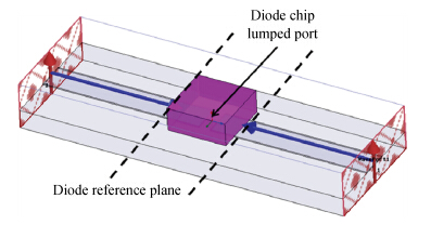
Diode chip model in HFSS.
SEMICONDUCTOR INTEGRATED CIRCUITS
Changfei Yao1, 2, , Ming Zhou2, Yunsheng Luo2 and Conghai Xu2
Corresponding author: Changfei Yao, Email: yaocf1982@163.com
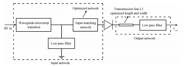
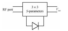
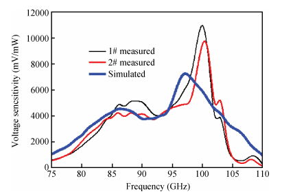
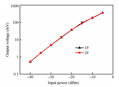
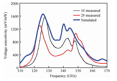
Abstract: Two broadband detectors at W-band and D-band are analyzed and designed with low barrier Schottky diodes. The input circuit of the detectors is realized by low and high impedance microstrip lines, and their output circuit is composed of a radio frequency (RF) bandstop filter and a tuning line for optimum reflection phase of the RF signal. S-parameters of the complete circuit are exported to a circuit simulator for voltage sensitivity analysis. For the W band detectors, the highest measured voltage sensitivity is 11800 mV/mW at 100 GHz, and the sensitivity is higher than 2000 mV/mW in 80-104 GHz. Measured tangential sensitivity (TSS) is higher than-38 dBm, and its linearity is superior than 0.99992 at 95 GHz. For the D band detector, the highest measured voltage sensitivity is 1600 mV/mW, and the typical sensitivity is 600 mV/mW in 110-170 GHz. TSS is higher than-29 dBm, and its linearity is superior than 0.99961 at 150 GHz.
Keywords: millimeter wave, zero bias Schottky diode, detector, voltage sensitivity
| [1] | |
| [2] | |
| [3] | |
| [4] | |
| [5] | |
| [6] | |
| [7] | |
| [8] | |
| [9] | |
| [10] | |
| [11] | |
| [12] | |
| [13] | |
| [14] | |
| [15] | |
| [16] | |
| [17] | |
| [18] | |
| [19] |

| [1] | |
| [2] | |
| [3] | |
| [4] | |
| [5] | |
| [6] | |
| [7] | |
| [8] | |
| [9] | |
| [10] | |
| [11] | |
| [12] | |
| [13] | |
| [14] | |
| [15] | |
| [16] | |
| [17] | |
| [18] | |
| [19] |


Article views: 4298 Times PDF downloads: 101 Times Cited by: 0 Times
Received: 13 August 2014 Revised: Online: Published: 01 June 2015
| Citation: |
Changfei Yao, Ming Zhou, Yunsheng Luo, Conghai Xu. Millimeter wave broadband high sensitivity detectors with zero-bias Schottky diodes[J]. Journal of Semiconductors, 2015, 36(6): 065002. doi: 10.1088/1674-4926/36/6/065002
****
C F Yao, M Zhou, Y S Luo, C H Xu. Millimeter wave broadband high sensitivity detectors with zero-bias Schottky diodes[J]. J. Semicond., 2015, 36(6): 065002. doi: 10.1088/1674-4926/36/6/065002.

|
| [1] | |
| [2] | |
| [3] | |
| [4] | |
| [5] | |
| [6] | |
| [7] | |
| [8] | |
| [9] | |
| [10] | |
| [11] | |
| [12] | |
| [13] | |
| [14] | |
| [15] | |
| [16] | |
| [17] | |
| [18] | |
| [19] |

 WeChat ID
Journal of Semiconductors © 2017 All Rights Reserved 京ICP备05085259号-2

 DownLoad: