


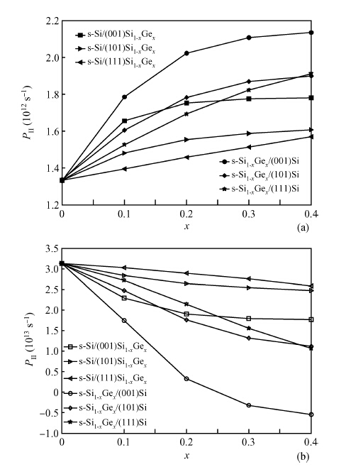
Fig. 2.
Relationship between the ionized impurity scattering rate and stress in Si-based strained materials when doping is (a) 1 $\times$ 10$^{17}$~cm$^{-3}$ and (b) 1 $\times$ 10$^{19}$ cm$^{-3}$.
SEMICONDUCTOR PHYSICS
Lixia Zhao1, 2, Chao Yang2, He Zhu2 and Jianjun Song2,
Corresponding author: Jianjun Song, E-mail: jianjun_79_81@xidian.edu.cn
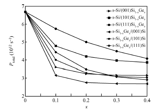
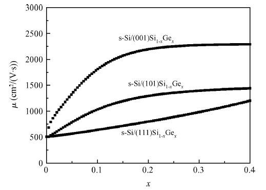
Abstract: Based on Fermi's golden rule and the theory of Boltzmann collision term approximation, the hole scattering mechanism related to stress and orientation in Si-based strained materials was studied in-depth. The results show that: (1) the total hole scattering rates in Si-based strained materials decrease obviously under strain; (2) the turn is Si/(111)Si1-xGex > Si/(101)Si1-xGex > Si1-xGex/(111)Si > Si1-xGex/(101)Si > Si/(001)Si1-xGex > Si1-xGex/(001)Si when Ge fraction is about 0.2; (3) the decreasing total hole scattering rates of in strained materials with the increasing stress is mainly caused the decreasing acoustic phonon scattering rate under strain. The theoretical conclusions obtained could provide important references for researching the hole mobility and the understanding of Si-based materials or other physical strained materials.
Keywords: strain, orientation, scattering, hole
| [1] | |
| [2] | |
| [3] | |
| [4] | |
| [5] | |
| [6] | |
| [7] | |
| [8] | |
| [9] | |
| [10] | |
| [11] | |
| [12] | |
| [13] | |
| [14] |
| [1] | |
| [2] | |
| [3] | |
| [4] | |
| [5] | |
| [6] | |
| [7] | |
| [8] | |
| [9] | |
| [10] | |
| [11] | |
| [12] | |
| [13] | |
| [14] |


Article views: 3065 Times PDF downloads: 12 Times Cited by: 0 Times
Received: 19 November 2014 Revised: Online: Published: 01 July 2015
| Citation: |
Lixia Zhao, Chao Yang, He Zhu, Jianjun Song. Scattering mechanism of hole in (001), (101), (111) biaxially-strained Si and Si1-xGex materials[J]. Journal of Semiconductors, 2015, 36(7): 072003. doi: 10.1088/1674-4926/36/7/072003
****
L X Zhao, C Yang, H Zhu, J J Song. Scattering mechanism of hole in (001), (101), (111) biaxially-strained Si and Si1-xGex materials[J]. J. Semicond., 2015, 36(7): 072003. doi: 10.1088/1674-4926/36/7/072003.

|
| [1] | |
| [2] | |
| [3] | |
| [4] | |
| [5] | |
| [6] | |
| [7] | |
| [8] | |
| [9] | |
| [10] | |
| [11] | |
| [12] | |
| [13] | |
| [14] |

 WeChat ID
Journal of Semiconductors © 2017 All Rights Reserved 京ICP备05085259号-2

 DownLoad:


