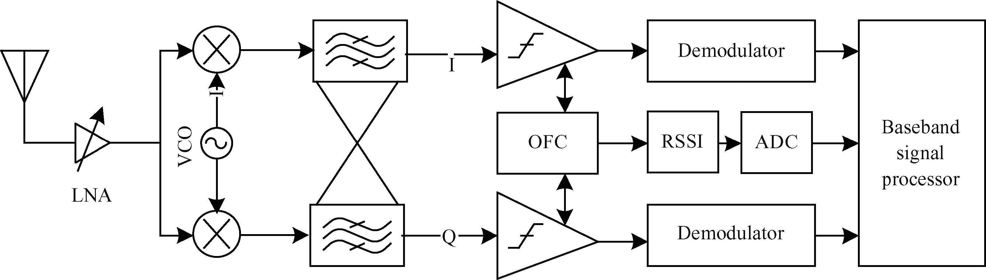
Loading [MathJax]/jax/output/HTML-CSS/jax.js
J. Semicond. > 2015, Volume 36 > Issue 8 > 085005

SEMICONDUCTOR INTEGRATED CIRCUITS

A CMOS high resolution, process/temperature variation tolerant RSSI for WIA-PA transceiver

Tao Yang, Yu Jiang, Jie Li, Jiangfei Guo, Hua Chen, Jingyu Han, Guiliang Guo and Yuepeng Yan

+ Author Affiliations

 Corresponding author: Tao Yang, Emailyangtao@ime.ac.cn

DOI: 10.1088/1674-4926/36/8/085005

PDF

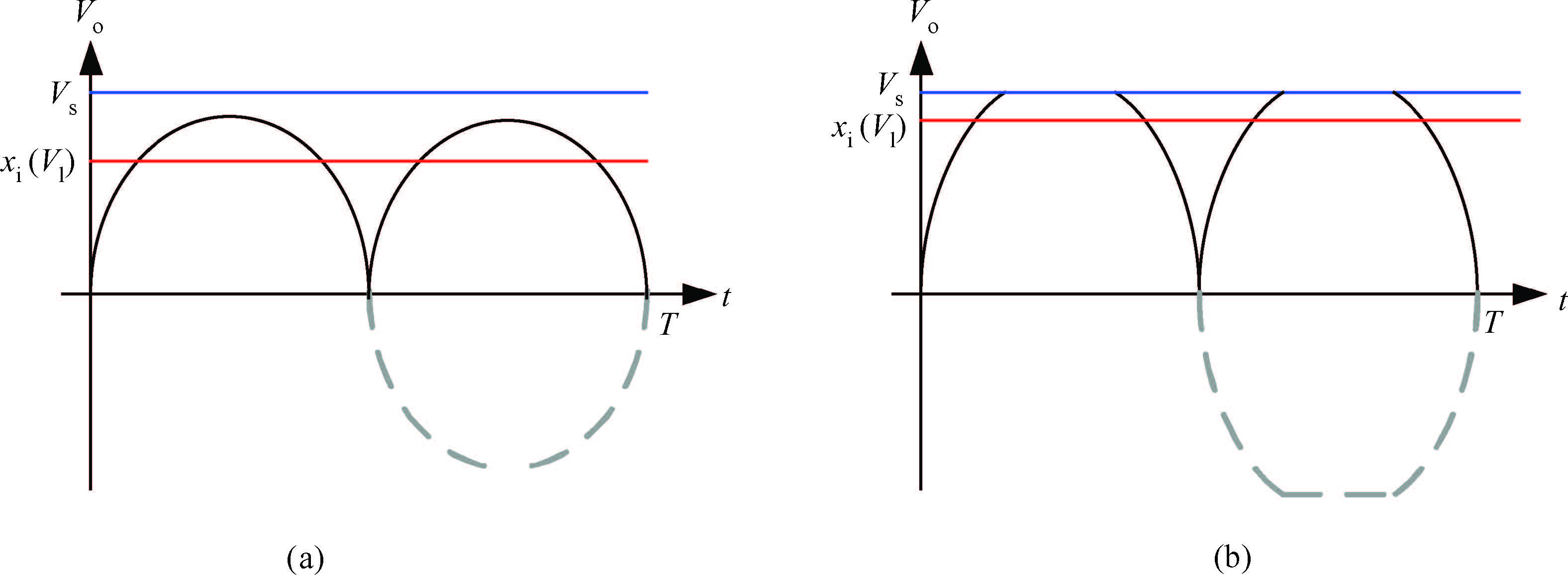
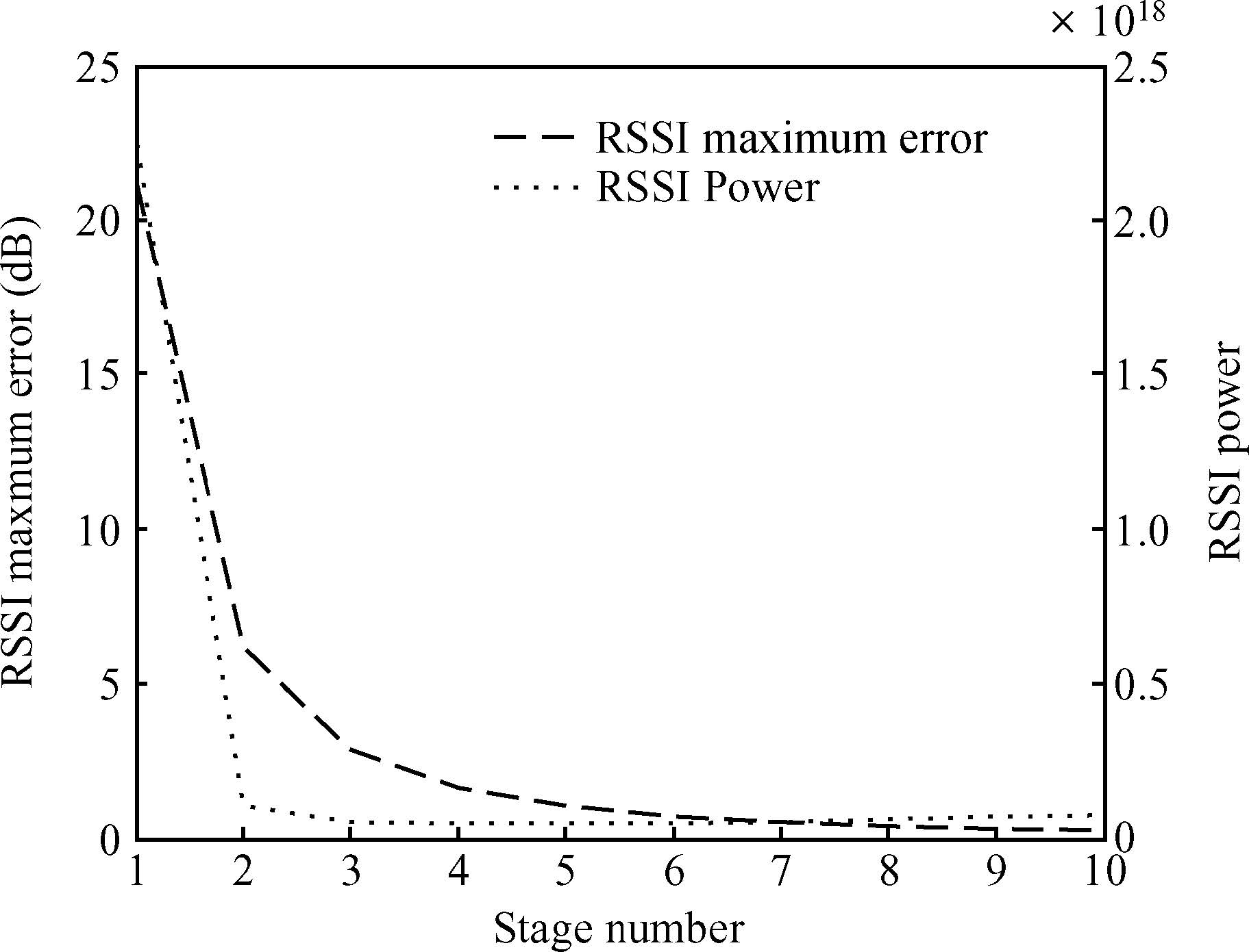
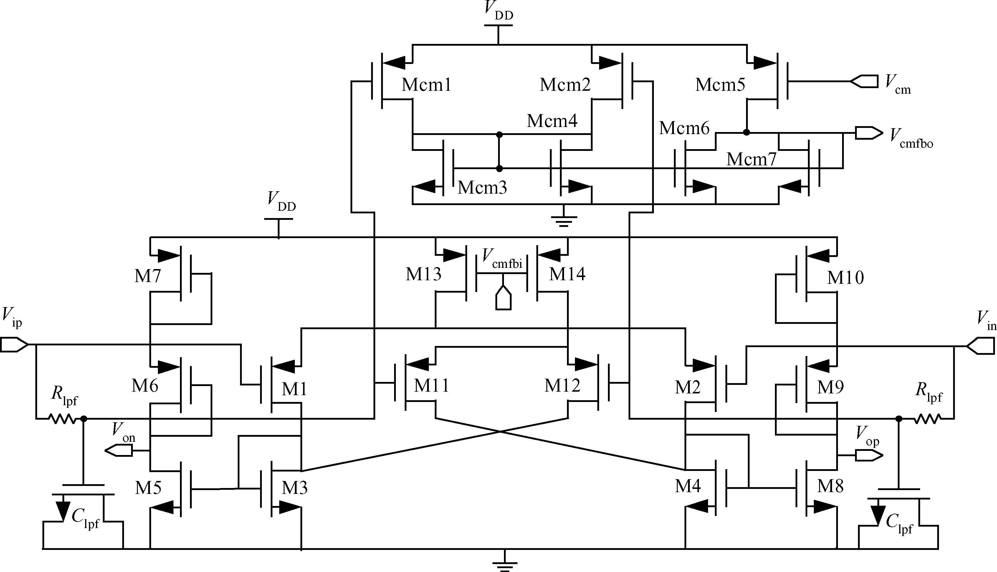
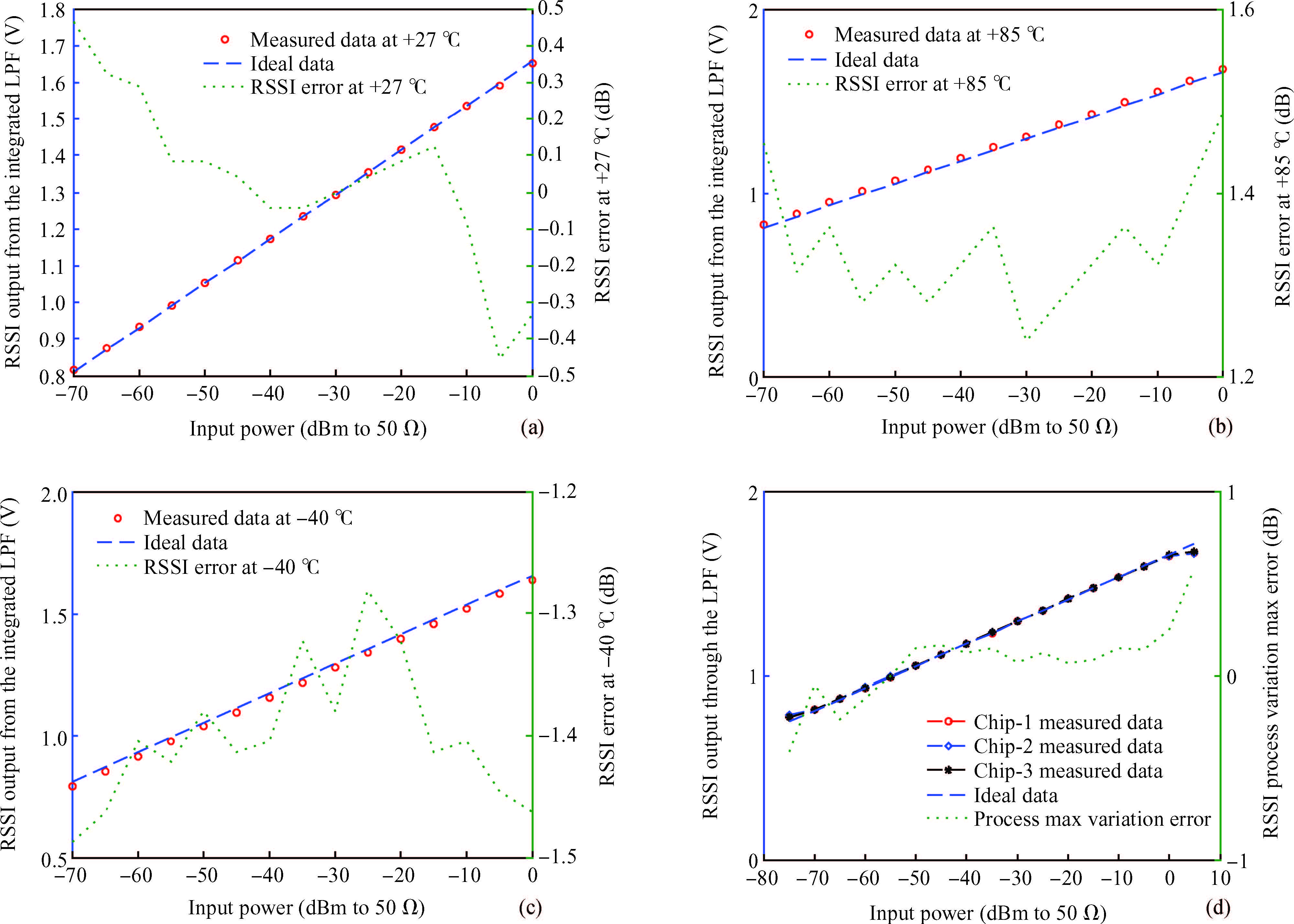
Abstract: This paper presents a high resolution, process/temperature variation tolerant received signal strength indicator (RSSI) for wireless networks for industrial automation process automation (WIA-PA) transceiver fabricated in 0.18μm CMOS technology. The active area of the RSSI is 0.24 mm2. Measurement results show that the proposed RSSI has a dynamic range more than 70 dB and the linearity error is within ± 0.5 dB for an input power from -70 to 0 dBm (dBm to 50 Ω ), the corresponding output voltage is from 0.81 to 1.657 V and the RSSI slope is 12.1 mV/dB while consuming all of 2 mA from a 1.8 V power supply. Furthermore, by the help of the integrated compensation circuit, the proposed RSSI shows the temperature error within ± 1.5 dB from -40 to 85 ℃, and process variation error within ± 0.25 dB, which exhibits good temperature-independence and excellent robustness against process variation characteristics.

Key words: limiterRSSIhigh resolutiondynamic rangedetection sensitivityrail-to-rail buffer

WIA-PA based on IEEE 802.15.4-2006[1, 2],is proposed by China for wireless industrial applications. Recently,470-510 MHz ISM band was released to the WIA-PA applications,for low-cost short-range applications. It employs GFSK modulation scheme and low-IF receiver architecture,so that the transceiver can be immune to low frequency problems such as flicker noise and DC offset. As shown in Figure 1,in the RF front-end,the complex channel-select filter down-converts RF signal to IF domain,rejects the image,and selects the desired channel. The limiter adjusts the amplitude of received IF signals to achieve a constant envelope. Therefore,it removes the AM noise and retains the frequency information. Linear amplification function is not needed because little information is on the amplitude with respect to the GFSK scheme.

Figure  Fig1.  Block diagram of a typical low-IF wireless receiver.

Compared with the VGA scheme,the RSSI block can handle a larger dynamic range while consuming less power and holding a simple circuitry. Normally,the RSSI represents the received signal power level and adjusts the gain of the RF front-end channel by the help of the baseband signal processor. Furthermore,the RSSI is used for localization in wireless sensor network systems[3, 4]. Resolution of the measured RSSI value affects the performance of the wireless communication system. Therefore,the RSSI circuit needs to be thoroughly analyzed and carefully designed[5, 6, 7]. Former works quantitatively derived the RSSI value but seldom considered the rectifier,low-pass filter (LPF)[8] and rail-to-rail buffer[9, 10]. These three blocks are essentially the critical building blocks of an RSSI circuit besides the limiter circuit and they should be taken into consideration carefully.

The RSSI circuit should meet a number of requirements,including low cost,low power,wide dynamic range (DR),high detection sensitivity and robust to PVT variations. Successive-detection architecture based on piecewise-linear approximation is adopted for realizing the logarithmic amplifier because the wide dynamic variation of the received signal can be represented within a limited indication range[11, 12, 13, 14, 15, 16]. It is essentially composed of several full-wave rectifiers and a low-pass filter,which are in combination with the proposed limiting amplifier circuits.

This paper is organized as follows. Section 2 analyzes the performance of RSSI theoretically and discusses the proposed RSSI architecture design. Section 3 describes circuit designs focusing on the proposed limiting amplifier,rectifier,LPF and rail-to-rail buffer circuits. The measurement results are shown in Section 4 and conclusions are given in Section 5.

Quantitative analyses of the RSSI circuit based on the successive detection architecture that the line in dB relationship between the narrow band modulated input signal level and the output voltage as well as the maximum deviation from an ideal logarithmic function[5, 6, 7] with a reasonable dynamic range and detection sensitivity are described completely. Successive-detection architecture has commonly been used because it is more accurate than the alternative structures based on PN-junctions. Also,a PN-junction-based logarithm amplifier has limited dynamic range and strong temperature dependency[13]. Meanwhile,some nonidealities such as AM-to-PM conversion[17],the output amplitude of limiting amplifier and common voltage effects,and so on,are also going to be considered.

Figure  Fig2.  Output voltage of each branch of the RSSI when (a) AiVIVs and (b) AiVI Vs for i = 0,1,,N.

The actual RSSI value is obtained by summing the output voltages from each branch in the successive detection architecture.

RSSI(VI)=Ni=0xi(VI),(1)
where N is the number of the limiter and xi(VI) is the output voltage of (i+1)th branch comprising of the rectifier and the LPF and it is the DC level of the saturated and rectified signal of AivI(t) where i= 0,1,,N,vI(t) is the input signal in time domain. So xi(VI) has two different ways depending on the magnitude of AiVI. Figure 2(a) shows AiVIVs and Figure 2(b) shows AiVI Vs for i= 0,1,,N. Vs is the saturated output voltage level,and A is the voltage gain of each limiting amplifier. For the continuous phase frequency modulated signal,xi(VI) does not depend on the modulated frequency but only on the amplitude VI,which means that the derived equations of the RSSI value,max error and dynamic range can be used for the frequency modulated signal such as GFSK. Only a narrow band phase-modulated signal has the same way that the RSSI value also depends on VI.

RSSI(VI)=ki=0xi(VI)|AiVIVs+Ni=k+1xi(VI)|AiVIVS=ki=02VIπAi+Ni=k+1{2VIπAi[11(VsAiVI)]+[12πsin1(VsAiVI)]Vs}.

(2)

To approximate the ideal logarithmic function accurately,the RSSI value should increase linearly as the amplitude of the input signal VI grows exponentially[6].

RSSI(VsAk)RSSI(VsAk+1)Vs,1kN2.

(3)

From Equation (3),the RSSI value adds Vs every time as VI is increased A times. So the ideal logarithmic RSSI curve can be represented by

RSSIideal(VI)=VslogA(VIVS)+NVS,VSAk+1VIVSAk,1kN1.

(4)

From Equations (2) and (3),the piece-wise linear RSSI curve can be represented by

RSSIapprox(VI)=Ak+1A1(VIVSAk+1)+(Nk1)VS,VSAk+1VIVSAk,1kN1.

(5)

As shown in Equation (5),besides VI,the RSSI value relates to the single-stage voltage gain and the saturated output voltage level of each limiting amplifier cell.

From Equations (4) and (5),the maximum RSSI error can be estimated when

|RSSIideal(VI)RSSIapprox(VI)|VI=0.

(6)

From Equations (4)-(6),the maximum RSSI error in dB mode can be obtained when

VI=VS(A1)Ak+1lnA.

(7)

Substitute Equation (7) in |RSSIideal(VI)RSSIapprox(VI)|,the maximum RSSI error in dB mode can be described as

RSSIerror,max,dB=10lnA×(lnA1lnA1lnA+1A1).

(8)

As shown in Equation (8),the RSSI error depends only on the single-stage voltage gain.

The RSSI dynamic range in dB mode can be obtained[7]

RSSIDR,dB=20log10A×{N+1logA[2A(20log10Aπ)2]}.

(9)

As shown in Equation (9),the RSSI dynamic range is determined by both the single stage voltage gain and the number of stages of a limiter.

The RSSI has a trade-off between dynamic range and detection sensitivity. The detection sensitivity can be obtained as

RSSIDS=RSSIapprox,maxRSSIapprox,minRSSIDR,dB.

(10)

The RSSI total power equals the sum of the single power of the limiter which is scalable to the power of the GBW,in other words,it is constrained by the dynamic range,maximum detection error and the bandwidth required by the systems.

RSSIpower,total=NPsN(A×Bs)2=N(A1NtBt21N1)2,(11)
where Bs,Bt and At are the single stage bandwidth,the total bandwidth and the total gain of limiting amplifier respectively. The single stage gain A,bandwidth Bs and noise are completely dependent on the circuit architecture which will be discussed and optimized to kill the PVT effects in the circuit analysis and design section. Once the overall gain At and bandwidth Bt of the limiting amplifier are specified,the voltage gain of each stage A is obviously reduced as the cascading number of the stage increases. However,this introduces more poles since the number of gain stage increases. The bandwidth of each stage Bs therefore has to be increased in order to maintain an overall bandwidth.

Figure  Fig3.  Linear error and power consumption versus gain stage numbers.

The effects of nonidealities are discussed below,which includes the A and Vs deviation and mismatch existing between different stages of the limiting amplifier,the residual DC offset with a DC offset cancellation method,the AM-to-PM conversion,the common mode voltage variation and the overall noise.

From Equation (5),the deviation of RSSI value due to A and Vs can be obtained by differentiating them severally. For simplicity and without of loss of generality,Equation (4) is chosen to analyze the variation.

begin{equation}
\begin{split}
{}
{\rm RSSI}_{\rm deviation}
=\frac{\partial {\rm RSSI}_{\rm ideal} (V_{\rm I})}{\partial A}\times \upDelta A+\frac{\partial {\rm ideal}_{\rm ideal} (V_{\rm I})}{\partial V_{\rm s}}\times \upDelta V_{\rm s}
\\
=V_{\rm s}\frac{\log_{\rm A} \left( \dfrac{V_{\rm s}}{V_{\rm I}}\right)}{\ln A}\times \frac{\upDelta A}{A}+V_{\rm s} \left[
N+\log_{\rm A} \left(\frac{V_{\rm I}}{V_{\rm s}} \right)-\frac{1}{\ln A}
 \right]
 \\
\quad  \times \frac{\upDelta V_{\rm s}}{V_{\rm s}}.
\end{split}
\end{equation}

(12)

From Equation (12),while VI decreases,the deviation of the RSSI value due to A variation increases,and while VI increases,the deviation of the RSSI value due to Vs variation decreases.

The transfer characteristic of each limiting amplifier will be affected if A and Vs mismatch exists between different stages. According to the successive detection architecture,the RSSI value is obtained by summing all the output voltage of each branch. So A and Vs can be approached using 1st order approximation as

Πik=0Ak=Ai(1+ik=0\upDeltaAkA),

(13)

Vs,i=Vs+\upDeltaVs,i=Vs(1+\upDeltaVs,iVs).

(14)

Meanwhile,the residual DC offset and the input noise limits the minimum input signal level. In other words,it may contaminate the dynamic range of RSSIDS. Voffset exists regardless of the signal amplitude,so the left part of RSSI value expression in Equation (2) can be modified for VIVoffset.

RSSI(VI)=1TT0|AivI(t)+Aivoffset(t)|dt=2πAiVI1(VoffsetVI)2+2πVoffsetsin1(VoffsetVI).

(15)
Figure  Fig4.  Architecture of the proposed RSSI.

The common mode voltage variation can be equivalent to DC offset.

The input-referred noise per unit bandwidth will be represented according to the proposed limiting amplifier next section. It also limits the minimum input signal power level.

There is another practical issue,which is the AM-to-PM conversion. This output phase modulation caused by input amplitude variation is mainly due to different delays of bandwidth-limited gain cell for different input levels. This phase variation will degrade the RSSI sensitivity. The phase variation can be expressed in terms of input signal band fin and total gain cell bandwidth as

\upDeltaϕ=17.6finBtN.

(16)

Shown in Figure 3 are linear error and power consumption versus gain stage numbers,which are obtained from Equations (8) and (11). Seven stages are the optimal number with all of 0.5 dB RSSI linear error and less power consumption. From Equation (16),in order to reduce the phase variation,Bt=10f_{\rm in}withf_{\rm in}$ = 1.5 MHz. From Equations (12) and (13),A ≥ 12 dB is evaluated to reduce the effects of A variation to total gain. From Equation (9),RSSI dynamic range RSSIDR,dB can be calculated to be about 80 dB. From Equations (12) and (14),the rail-to-rail output circuit is used to reduce the Vs variation. From Equation (15),an optimal input signal level should be twice the input-referred DC offset with the help of powerful DC-offset loop and noise-cancelled mechanics. Once the limiting architecture is proposed with the Vs,the detection sensitivity RSSIDS is chosen about 12 mV/dB. The above calculated and simulated results are used as the initial parameters to reduce the designing iterative process of RSSI.

As shown in Figure 4,a general RSSI circuit based on the successive detection architecture consists of the cascade of N limiting amplifier cell,of which voltage gain is A and saturated output voltage level is Vs,plus N+ 1 rectifiers,an LPF and a rail-to-rail buffer.

Two-path I/Q RSSI structure is adopted to reduce the output voltage glitch[19] and the chip area rapidly. The residual harmonic components are sufficiently attenuated by the small on-chip RC filter. In traditional single path RSSI,the output current of the full-wave current rectifier includes the second-order harmonic component as shown in Equation (17). Therefore,large capacitance is needed to filter the output voltage ripple. According to Equation (18),the second-order harmonic component of the output current can be ideally cancelled.

ITotal1p=sin2(ωt)=1212cos(2ωt),

(17)

ITotal2p=sin2(ωt)+cos2(ωt)=1.

(18)

The limiting amplifier is basically an amplifier chain that enlarges different magnitudes of input signal into saturation. This amplifier chain has to provide a small signal gain of at least 80 dB in order to cover the required input dynamic range in WIA-PA application. Meanwhile,it has to yield a high-pass function with the help of DC extraction,DCOC and CMFB circuits at each stage to alleviate the dc offset due to mismatch,variation and residue of DC value maximally. The designed upper bandwidth is ten times that of the IF 1.5-MHz in order to reduce the AM-PM conversion effect,while the lower band is set at 100 kHz which causes little influence on data band near IF. Each section of the rectifier is obtained by rectifying each gain cell output of the limiting amplifier. The sum of the output of the cascaded section with a low pass filter is used to measure the signal strength.

Figure  Fig5.  Circuit diagram of the gain stage with feed-forward offset cancellation and CMFB functions.

A pseudo differential structure always suffers from path mismatch. It is more severe in a high gain device,because the accumulated offset in the front stage may smear the input small signal and generate a wrong saturated output voltage in the following gain stage[14],and in order to avoid driving the diode load into velocity saturation region,the proposed circuit employs cascaded diode connected transistors load[20]. To avoid the offset being amplified,a feed forward type offset cancellation method[21] is applied as shown in Figure 5. The offset in the previous stage which is extracted by an RC network will be subtracted from the input signal by the cross-connected pair M11 and M12 in the current stage. The frequency response of this gain stage with the help of the small signal analysis can be derived as

Av=ADC×HBPF(s)=gm1,2gm6,9+gm7,10×sRlpfClpf(sRlpfClpf+1)(sCPOgm6,9+gm7,10+1),(19)
where CPO represents the parasitic capacitance of the output node,gm1,2,gm6,9 and gm7,10 are the trans-conductance of the transistor M1,M2,M6,M9 and M7,M10. Rlpf,Clpf are the components of the DC abstract circuit.

The pseudo-differential structure has poor common mode behavior. The output common level fluctuation will be reduced by a factor of the loop gain with the help of a common mode feedback (CMFB) circuit. Directly applying the DC information from the previous extraction circuit as the output common mode voltage does not cause additional parasitic capacitance at the output node. Moreover,no extra power will be consumed. The sensed common mode voltage is compared with a reference voltage Vcm. The error signal is amplified and fed back to the bias circuit M13 and M14 of the gain stage[14].

From Figure 5,the input-referred noise per unit bandwidth can be represented as

V2v=8kTγ(gm1+gm3+gm5+gm6+gm7)(gm6+gm7)4(gm1gm6gm7)2.

(20)

From Equation (20),increasing gm1 can reduce noise effectively. The flick noise can be ignored with the LPF circuit.

The simulation result of the limiter is shown in Figure 6. The frequency response of the limiter with forward offset cancellation circuit shows the band-pass function with about 88~dB total gain and 12 MHz bandwidth.

Figure  Fig6.  Frequency response of the limiter with offset cancellation circuit.
Figure  Fig7.  Circuit diagram of the proposed full-wave rectifier.

As shown in Figure 7,the proposed output current programmable full-wave rectifier consists of doubled unbalanced source-coupled pairs with the cross-coupled input stage and parallel-connected output stage. The proposed full-wave rectifier is more precise and smooth compared to the traditional full-wave rectifier[11],which is proved by the measurement results. As shown in Equation (21),the output current of the full-wave current rectifier is a function of the reference bias current and the input signal[22]. The programmable reference bias current controls the tradeoff between the dynamic range and detection sensitivity of RSSI. Here,the reference (1x) current is compensated with a replica biasing circuit for PVT variations.

VRSSI=(Il+IQ)×Rpull_up=(xi(VII)+xq(VIQ))×Rpull_up=[f(VII+At×Iprogramblebias)+f(VIQ+At×Iprogramblebias)]×Rpull_up,(21)
where Rpull_up is the PULL UP register as shown in Figure~8.

Figure  Fig8.  Proposed LPF and buffer.

Besides the programmable reference (1x) current mirror,the transfer curve of the RSSI keeps stable under various PVT variations further with the help of the self-adaptive bias circuit by reducing the effects of the Rpull_up of the LPF which is shown at the top right corner of Figure 7. The programmable IBIAS will be changed with the Vref pad. So Equation (21) can be modified as

VRSSI=[f(VII+At×VDDVrefRpull_up)+f(VIQ+At×VDDVrefRpull_up)]×Rpull_up=[f(VII+At×(VDDVref))+f(VIQ+At×(VDDVref))].

(22)

The bandwidth of the LPF should be much lower than the frequency of the input signal and the stop band attenuation is larger to reduce ripples on the real RSSI value. As shown in Figure 8,a passive RC filter with two poles is provided[8]. The LPF and rectifier comprises the summer which should have the same weighting factor for each branch.

Usually,the RSSI output value is used as the input of ADC which has large capacitance at the input node. Meanwhile,the RSSI value has a wide range and in order not to sacrifice the dynamic range of RSSI,as shown in Figure 8,a constant-gm op-amp with rail-to-rail input and output-stage-based buffer is added between them.

As shown in Figure 8,the constant-gm input stage of the proposed two-stage op-amp is based on the configuration that consists of four MOSFETS M2,M3,M6,M7 as dummy differential pairs to select a different differential pair M1,M4,M5,M8 as input pair,according to the different common-mode voltage VB[10] which can range from VSS to VDD for the rail-to-rail input stage. To obtain the constant gm,In=Ip,μnCoxWL=μCoxWL. However,when the difference between the VB and the common mode voltage Vcm is small,the variation will be raised. So,the sizes of the dummy MODFETS can be set three times greater than the corresponding differential input pairs. In addition,a class-AB output stage is employed to obtain a wide output range[9]. The purpose of the class-AB control circuit is to prevent the output transistors or any other transistors in the circuit from switching off,as this would deteriorate the step response of the stage[10]. To reduce noise and offset,the class-AB driver circuit M19,M20 which biased by the M22,M25 has been incorporated in the folded-cascaded summing circuit M11-M18 of the rail-to-rail input stage. The amplifier is compensated using two split miller capacitors between the output stage M27,M28 and current mirrors.

The simulation result shows that the proposed op-amp has a constant gm within 4.5{\%} and consumes all of 200 μA with the real ADC load.

Based on the structure shown in Figure 4,this proposed high resolution,process/temperature variation tolerant RSSI is fabricated in the TSMC 0.18 μm 1P6M RF CMOS technology and draws no more than 2 mA from a 1.8 V power supply. The chip microphotograph of the RSSI is shown in Figure 9. Its active area is 0.24 mm2.

Figures 10(a)-10(c) display the RSSI value and its maximum error in dB mode with the dynamic range of input signal power from 70 to 0 dBm (to 50 \upOmega) at +27,40 and +85~\du respectively. Figure 10(d) compares the process variation in dB mode of different chips on the same wafer at the same temperature.

Figure  Fig9.  Chip microphotograph of the proposed RSSI.

Depending on the proposed RSSI circuits and rational modified circuits,such as self-adaptive bias and 1 : 1 programmable current mirrors,the proposed RSSI exhibits good temperature-independence and excellent robustness against process variation characteristics which matches well with the theoretical analysis.

Figure  Fig10.  Measured RSSI output with temperature variation and process variation. (a) Measured RSSI output data and its error at 27 \du. (b) Measured RSSI output data and its error at 85 \du. (c) Measured RSSI output data and its error at 40 \du. (c) Compare the different chips for process variation.

As shown in Figures 10(a),10(b),10(c),the maximum errors in dB mode are within (0.5 dB,+0.5 dB) at 27 \du,within (+1.2 dB,+1.3 dB) at +85 \du and within (1.5 dB,12.5 dB) at 40 \du respectively. So,total RSSI temperature error is within (1.5 dB,+1.3 dB) from 40 to +85 \du with 70 dB dynamic range. Figure 10(d) shows the process variation error is within (0.25 dB,+0.25 dB) from 70 to 0 dBm. The corresponding output voltage is from 0.81 to 1.657 V and the RSSI slope is 12.1 mV/dB while consuming all of 2 mA from a 1.8 V power supply.

Table  1.  Comparison of different RSSIs performance.
DownLoad: CSV  | Show Table

The comparison of different RSSIs performance is shown in Table 1. According to the spec of WIA-PA,the proposed RSSI has the optimization results.

In this paper,a high resolution,process/temperature variation tolerant received signal strength indicator (RSSI) for WIA-PA receiver is proposed. To achieve robust performance under 1.8 V operation by a standard TSMC 0.18 μm 1P6M RF CMOS technology,a novel RSSI circuit based on the successive detection I/Q architecture is proposed with the help of the theoretical analysis of the value level,dynamic range,detection sensitivity,maximum variation error and non-ideal effects of RSSI including the LPF. In order to improve the performance of the RSSI,a novel gain stage with feed-forward offset cancellation and common mode feedback mechanism is proposed and followed by a doubled unbalanced source-coupled pairs rectifier which is finer than a traditional one. Considering the characteristic of RSSI and usage as input of followed ADC which has a large capacitor at the input node,a constant-gm rail-to-rail op-amp buffer is proposed at last. Depending on the proposed RSSI circuits and rational modified circuits such as self-adaptive bias and 1 : 1 programmable current mirrors,etc.,the proposed RSSI exhibits good temperature-independence and excellent robustness against process variation characteristics. Measurement results show that the proposed RSSI has a dynamic range more than 70 dB and the maximum linearity error is within ±0.5 dB for an input power from 70 to 0 dBm (dBm to 50 \upOmega),the corresponding output voltage is from 0.81 to 1.657 V and the RSSI slope is 12.1 mV/dB while consuming all of 2 mA from a 1.8 V power supply. Furthermore,by the help of the integrated compensation circuit,the proposed RSSI shows the temperature error within ±1.5 dB from 40 to 85~\du,and process variation error within ±0.25 dB.

The author wishes to thank Yan Yuepeng for valuable discussions on the system and block design of the RSSI. The author is also indebted to Li Jie,Liu Shengyou and Guo Guiliang for the support of the chip test.


[1]
[2]
[3]
[4]
[5]
[6]
[7]
[8]
[9]
[10]
[11]
[12]
[13]
[14]
[15]
[16]
[17]
[18]
[19]
[20]
[21]
[22]
Fig1.  Block diagram of a typical low-IF wireless receiver.

Fig2.  Output voltage of each branch of the RSSI when (a) AiVIVs and (b) AiVI Vs for i = 0,1,,N.

Fig3.  Linear error and power consumption versus gain stage numbers.

Fig4.  Architecture of the proposed RSSI.

Fig5.  Circuit diagram of the gain stage with feed-forward offset cancellation and CMFB functions.

Fig6.  Frequency response of the limiter with offset cancellation circuit.

Fig7.  Circuit diagram of the proposed full-wave rectifier.

Fig8.  Proposed LPF and buffer.

Fig9.  Chip microphotograph of the proposed RSSI.

Fig10.  Measured RSSI output with temperature variation and process variation. (a) Measured RSSI output data and its error at 27 \du. (b) Measured RSSI output data and its error at 85 \du. (c) Measured RSSI output data and its error at 40 \du. (c) Compare the different chips for process variation.

DownLoad: CSV
DownLoad: CSV
DownLoad: CSV
DownLoad: CSV

Table 1.   Comparison of different RSSIs performance.

DownLoad: CSV
[1]
[2]
[3]
[4]
[5]
[6]
[7]
[8]
[9]
[10]
[11]
[12]
[13]
[14]
[15]
[16]
[17]
[18]
[19]
[20]
[21]
[22]
1

A high sensitive 66 dB linear dynamic range receiver for 3-D laser radar

Rui Ma, Hao Zheng, Zhangming Zhu

Journal of Semiconductors, 2017, 38(8): 085006. doi: 10.1088/1674-4926/38/8/085006

2

Detection of lead ions with AlGaAs/InGaAs pseudomorphic high electron mobility transistor

Jiqiang Niu, Yang Zhang, Min Guan, Chengyan Wang, Lijie Cui, et al.

Journal of Semiconductors, 2016, 37(11): 114003. doi: 10.1088/1674-4926/37/11/114003

3

Design and test of a capacitance detection circuit based on a transimpedance amplifier

Linfeng Mu, Wendong Zhang, Changde He, Rui Zhang, Jinlong Song, et al.

Journal of Semiconductors, 2015, 36(7): 075007. doi: 10.1088/1674-4926/36/7/075007

4

Dynamic threshold voltage operation in Si and SiGe source junctionless tunnel field effect transistor

Shibir Basak, Pranav Kumar Asthana, Yogesh Goswami, Bahniman Ghosh

Journal of Semiconductors, 2014, 35(11): 114001. doi: 10.1088/1674-4926/35/11/114001

5

A 14-bit 1-GS/s DAC with a programmable interpolation filter in 65 nm CMOS

Qi Zhao, Ran Li, Dong Qiu, Ting Yi, Yang Liu Bill, et al.

Journal of Semiconductors, 2013, 34(2): 025004. doi: 10.1088/1674-4926/34/2/025004

6

A wideband large dynamic range and high linearity RF front-end for U-band mobile DTV

Rongjiang Liu, Shengyou Liu, Guiliang Guo, Xu Cheng, Yuepeng Yan, et al.

Journal of Semiconductors, 2013, 34(10): 105003. doi: 10.1088/1674-4926/34/10/105003

7

A voltage regulator system with dynamic bandwidth boosting for passive UHF RFID transponders

Jinpeng Shen, Xin'an Wang, Shan Liu, Shoucheng Li, Zhengkun Ruan, et al.

Journal of Semiconductors, 2013, 34(10): 105004. doi: 10.1088/1674-4926/34/10/105004

8

A CMOS low power, process/temperature variation tolerant RSSI with an integrated AGC loop

Qianqian Lei, Min Lin, Yin Shi

Journal of Semiconductors, 2013, 34(3): 035007. doi: 10.1088/1674-4926/34/3/035007

9

A high dynamic range linear RF power detector with a preceding LNA

Dai Yingbo, Han Kefeng, Yan Na, Tan Xi

Journal of Semiconductors, 2012, 33(1): 015005. doi: 10.1088/1674-4926/33/1/015005

10

Chaotic dynamics dependence on doping density in weakly coupled GaAs/AlAs superlattices

Yang Gui, Li Yuanhong, Zhang Fengying, Li Yuqi

Journal of Semiconductors, 2012, 33(9): 092002. doi: 10.1088/1674-4926/33/9/092002

11

A process/temperature variation tolerant RSSI

Lei Qianqian, Lin Min, Shi Yin

Journal of Semiconductors, 2012, 33(12): 125010. doi: 10.1088/1674-4926/33/12/125010

12

MOS Capacitance-Voltage Characteristics II. Sensitivity of Electronic Trapping at Dopant Impurity from Parameter Variations

Jie Binbin, Sah Chihtang

Journal of Semiconductors, 2011, 32(12): 121001. doi: 10.1088/1674-4926/32/12/121001

13

A 1-V 60-μW 85-dB dynamic range continuous-time third-order sigma–delta modulator

Li Yuanwen, Qi Da, Dong Yifeng, Xu Jun, Ren Junyan, et al.

Journal of Semiconductors, 2009, 30(12): 125011. doi: 10.1088/1674-4926/30/12/125011

14

A 540-W digital pre-amplifier with 88-dB dynamic range for electret microphones

Liu Yan, Hua Siliang, Wang Donghui, Hou Chaohuan

Journal of Semiconductors, 2009, 30(5): 055004. doi: 10.1088/1674-4926/30/5/055004

15

A high precision programmable bandgap voltage reference design for high resolution ADC

Zhu Tiancheng, Yao Suying, Li Binqiao

Journal of Semiconductors, 2009, 30(7): 075005. doi: 10.1088/1674-4926/30/7/075005

16

A Novel Capacitive Biaxial Microaccelerometer Based on the Slide-Film Damping Effect

Dong Linxi, Yan Haixia, Qian Xian, Sun Lingling

Journal of Semiconductors, 2008, 29(2): 219-223.

17

A 0.5mV High Sensitivity 200Mbps CMOS Limiting Amplifier with RSSI for Optical Receivers

Wang Rong, Wang Zhigong, Xu Jian, Guan Zhiqiang

Journal of Semiconductors, 2008, 29(2): 262-268.

18

A New CMOS Image Sensor with a High Fill Factor and the Dynamic Digital Double Sampling Technique

Liu Yu, Wang Guoyu

Chinese Journal of Semiconductors , 2006, 27(2): 313-317.

19

A Current-Mode DC-DC Buck Converter with High Stability and Fast Dynamic Response

Chen Dongpo, He Lenian, Yan Xiaolang

Chinese Journal of Semiconductors , 2006, 27(10): 1742-1749.

20

High-Integrated-Photosensitivity Negative-Electron-Affinity GaAs Photocathodes with Multilayer Be-Doping Structures

Wang Xiaofeng, Zeng Yiping, Wang Baoqiang, Zhu Zhanping, Du Xiaoqing, et al.

Chinese Journal of Semiconductors , 2005, 26(9): 1692-1698.

1. Wang, Y., Diao, S., Lin, F. et al. An Ultra-Low Power Subthreshold CMOS RSSI for Wake-Up Receiver. Journal of Circuits, Systems and Computers, 2016, 25(8): 1650090. doi:10.1142/S0218126616500900
  • Search

    Advanced Search >>

    GET CITATION

    Tao Yang, Yu Jiang, Jie Li, Jiangfei Guo, Hua Chen, Jingyu Han, Guiliang Guo, Yuepeng Yan. A CMOS high resolution, process/temperature variation tolerant RSSI for WIA-PA transceiver[J]. Journal of Semiconductors, 2015, 36(8): 085005. doi: 10.1088/1674-4926/36/8/085005
    T Yang, Y Jiang, J Li, J F Guo, H Chen, J Y Han, G L Guo, Y P Yan. A CMOS high resolution, process/temperature variation tolerant RSSI for WIA-PA transceiver[J]. J. Semicond., 2015, 36(8): 085005. doi: 10.1088/1674-4926/36/8/085005.
    shu

    Export: BibTex EndNote

    Article Metrics

    Article views: 2727 Times PDF downloads: 24 Times Cited by: 1 Times

    History

    Received: 19 January 2015 Revised: Online: Published: 01 August 2015

    Catalog

      Email This Article

      User name:
      Email:*请输入正确邮箱
      Code:*验证码错误
      Tao Yang, Yu Jiang, Jie Li, Jiangfei Guo, Hua Chen, Jingyu Han, Guiliang Guo, Yuepeng Yan. A CMOS high resolution, process/temperature variation tolerant RSSI for WIA-PA transceiver[J]. Journal of Semiconductors, 2015, 36(8): 085005. doi: 10.1088/1674-4926/36/8/085005 ****T Yang, Y Jiang, J Li, J F Guo, H Chen, J Y Han, G L Guo, Y P Yan. A CMOS high resolution, process/temperature variation tolerant RSSI for WIA-PA transceiver[J]. J. Semicond., 2015, 36(8): 085005. doi: 10.1088/1674-4926/36/8/085005.
      Citation:
      Tao Yang, Yu Jiang, Jie Li, Jiangfei Guo, Hua Chen, Jingyu Han, Guiliang Guo, Yuepeng Yan. A CMOS high resolution, process/temperature variation tolerant RSSI for WIA-PA transceiver[J]. Journal of Semiconductors, 2015, 36(8): 085005. doi: 10.1088/1674-4926/36/8/085005 ****
      T Yang, Y Jiang, J Li, J F Guo, H Chen, J Y Han, G L Guo, Y P Yan. A CMOS high resolution, process/temperature variation tolerant RSSI for WIA-PA transceiver[J]. J. Semicond., 2015, 36(8): 085005. doi: 10.1088/1674-4926/36/8/085005.

      A CMOS high resolution, process/temperature variation tolerant RSSI for WIA-PA transceiver

      DOI: 10.1088/1674-4926/36/8/085005
      Funds:

      Project supported by the National High Technology Research and Development Program of China (No. 2011AA040102).

      More Information
      • Corresponding author: Emailyangtao@ime.ac.cn
      • Received Date: 2015-01-19
      • Accepted Date: 2015-02-09
      • Published Date: 2015-01-25

      Catalog

        /

        DownLoad:  Full-Size Img  PowerPoint
        Return
        Return