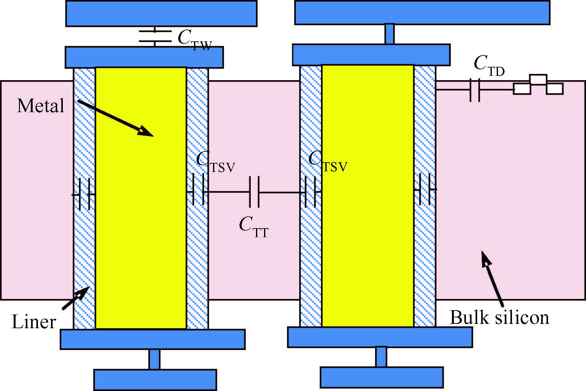
Processing math: 100%
J. Semicond. > 2015, Volume 36 > Issue 8 > 085006

SEMICONDUCTOR INTEGRATED CIRCUITS

An efficient method for comprehensive modeling and parasitic extraction of cylindrical through-silicon vias in 3D ICs

Qiang Yao1, Zuochang Ye1 and Wenjian Yu2,

+ Author Affiliations

 Corresponding author: Wenjian Yu, Emailyu-wj@tsinghua.edu.cn

DOI: 10.1088/1674-4926/36/8/085006

PDF

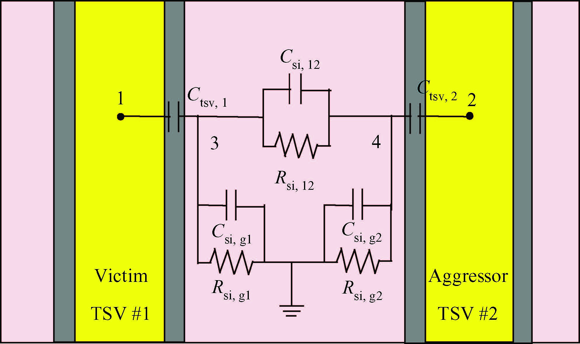
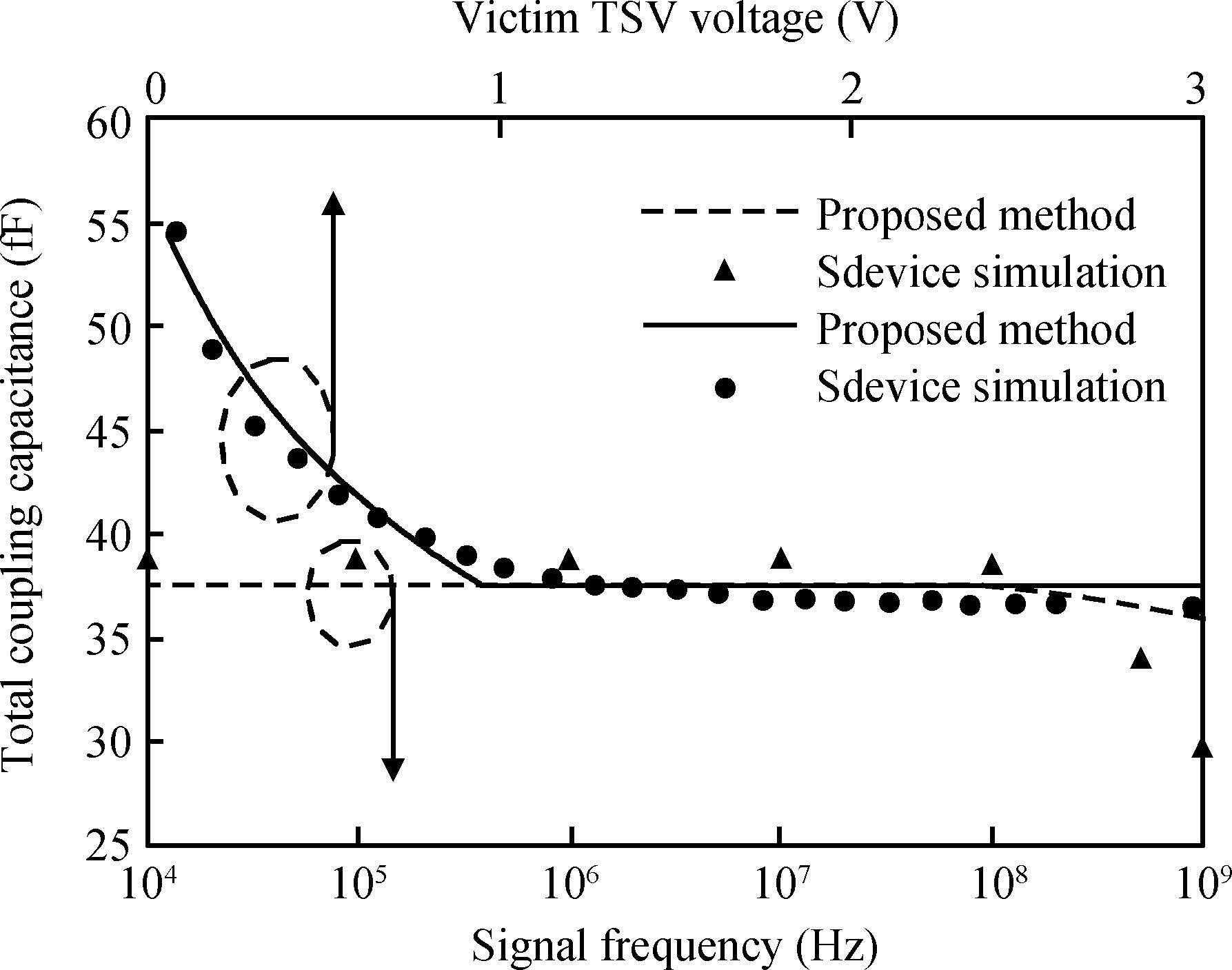
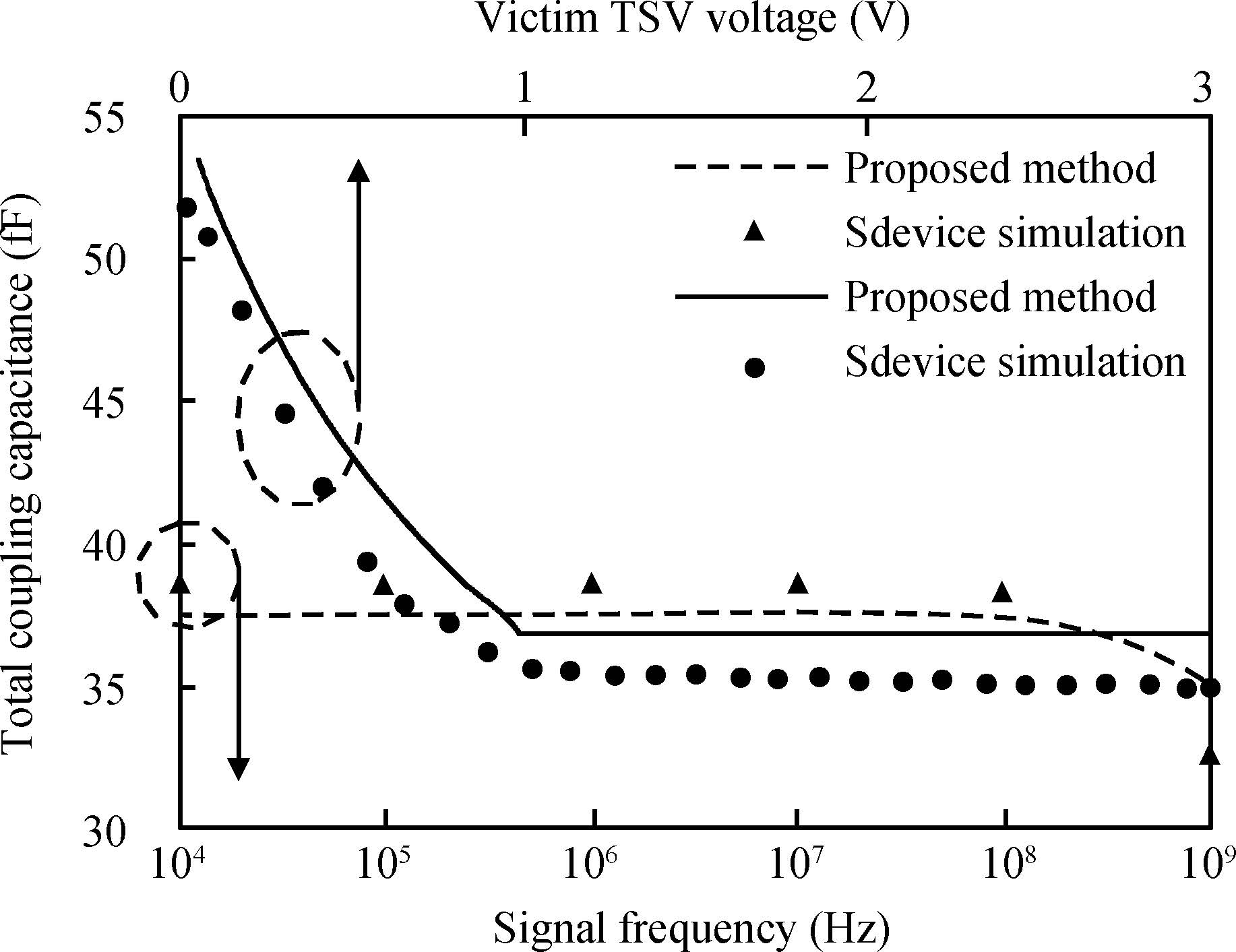
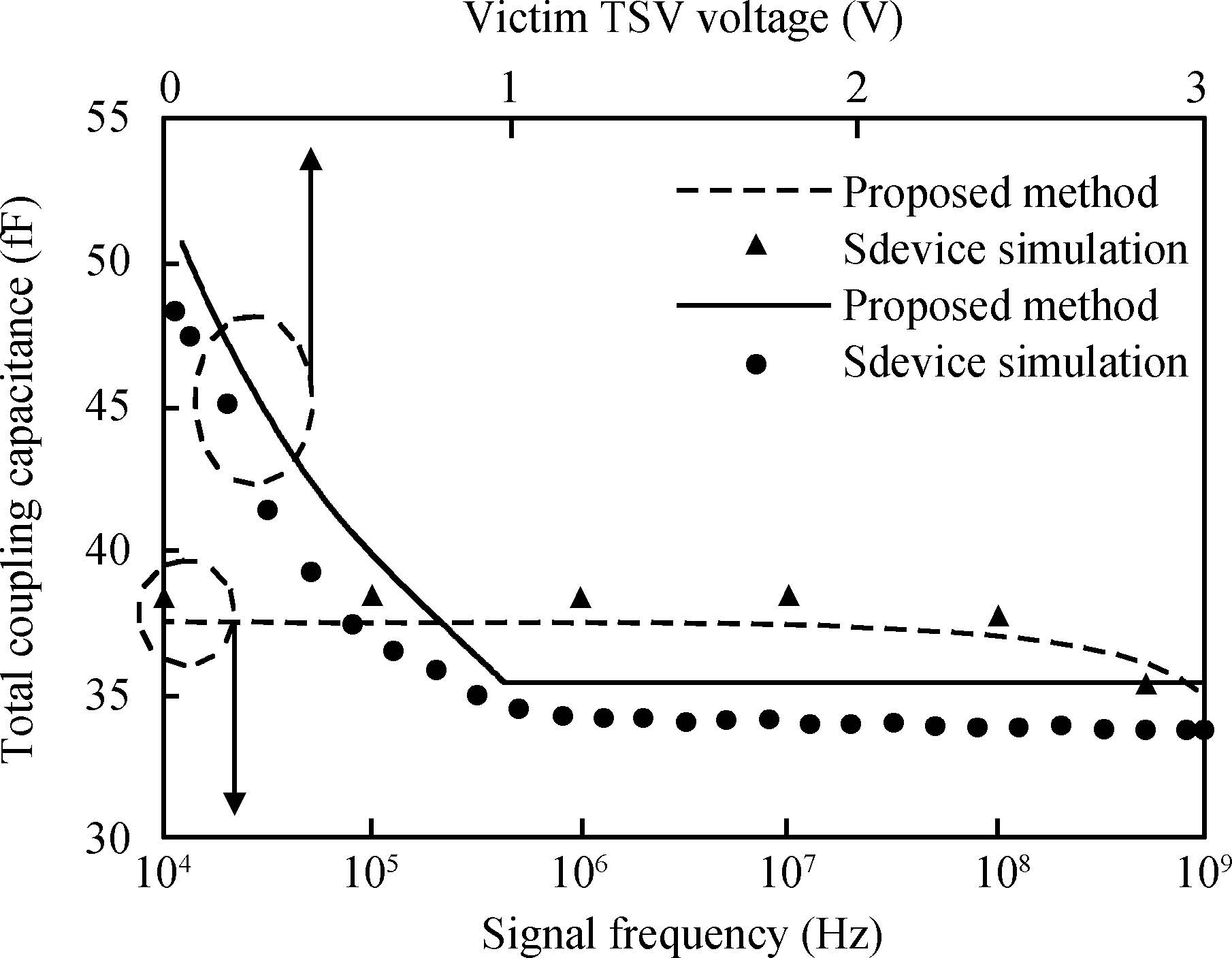
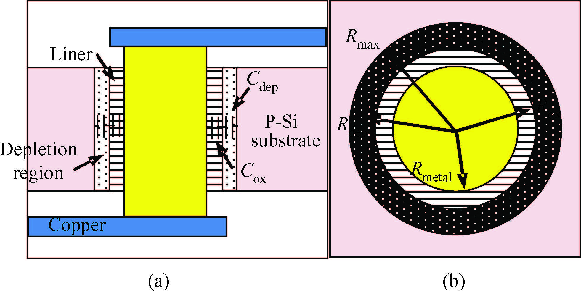
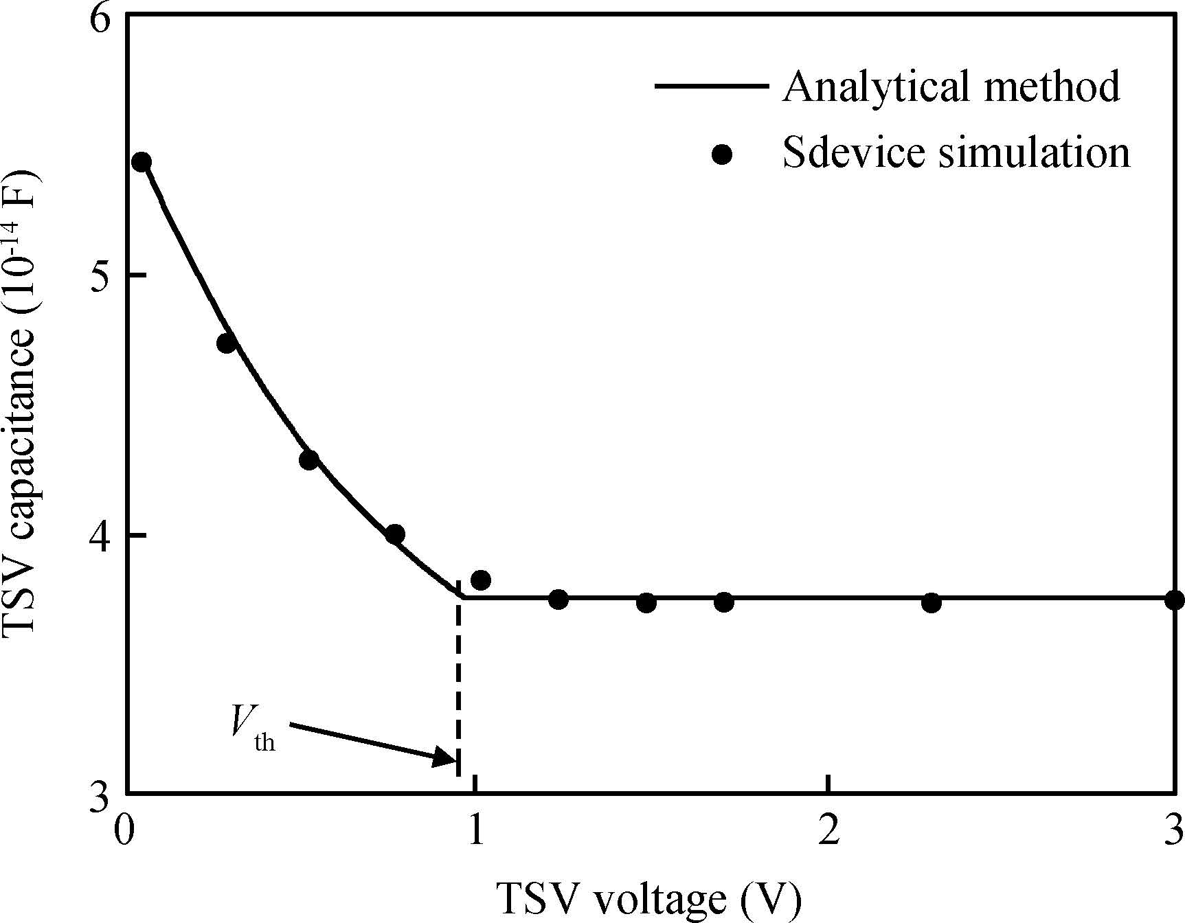
Abstract: To build an accurate electric model for through-silicon vias (TSVs) in 3D integrated circuits (ICs), a resistance and capacitance (RC) circuit model and related efficient extraction technique are proposed. The circuit model takes both semiconductor and electrostatic effects into account, and is valid for low and medium signal frequencies. The electrostatic capacitances are extracted with a floating random walk based algorithm, and are then combined with the voltage-dependent semiconductor capacitances to form the equivalent circuit. Compared with the method used in Synopsys's Sdevice, which completely simulates the electro/semiconductor effects, the proposed method is more efficient and is able to handle the general TSV layout as well. For several TSV structures, the experimental results validate the accuracy of the proposed method for the frequency range from 10 kHz to 1 GHz. The proposed method demonstrated 47× speedup over the Sdevice for the largest 9-TSV case.

Key words: 3D ICthrough silicon via (TSV)parasitic extractionfloating random walk algorithmmetal-oxide-semiconductor (MOS) capacitance

Three-dimensional integrated circuits (3D ICs) are generally considered to be one of the most prominent solutions that offer a way beyond Moore's law. A through-silicon via (TSV) is a popular choice for the vertical signal connection in 3D ICs and it is compatible with current process technologies. Some IC products,such as CMOS image sensors,have been manufactured using the TSV based 3D IC technology. The 3D IC technology will be applied to more commercial products.

The accurate extraction of resistance and capacitance (RC) parasitics of TSVs is essential in studying the performance and power consumption of 3D ICs. It is important for both the design-time circuit optimization,and the performance verification guaranteeing a reasonable production yield. Because TSVs across two IC tiers penetrate the silicon substrate,there is a kind of cylindrical metal-oxide-semiconductor (MOS) capacitor around the TSV,in addition to the conventional electrostatic capacitances among metal wires. As shown in Figure 1,CTSV between a TSV and its surrounding silicon stands for the MOS capacitance,while other capacitance components belong to the conventional electrostatic capacitance. To accurately model the parasitic effects of TSV,all these capacitance components should be considered. This requires a comprehensive treatment to the semiconductor effect and electrostatic field. Field-solver simulators,such as the Sdevice of Synopsys[1],is able to perform a complete extraction of the TSV structure,and produce accurate capacitance results. However,this kind of field solver employs an electromagnetic finite element method (FEM),and costs huge runtime and memory usage.

Figure  Fig1.  Cross-section view of TSVs and conventional interconnect wires in a 3D IC.

In Reference [2],the RLC parameters of the TSV were modeled as functions of physical parameters and metal characteristics. However,only one TSV was considered for modeling the semiconductor effect in MOS capacitance,with effects from surrounding TSVs ignored. In Reference [3],an equivalent circuit model was built for a 2-TSV layout structure. The method cannot be extended to the scenario with multiple TSVs. A model considering multiple TSVs was proposed based on the multi-conductor transmission line theory in Reference [4]. However,the silicon depletion region around the TSV was ignored in that work. In References [5, 6, 7, 8],the focus is on the electrostatic capacitance among ITVs and horizontal wires,instead of the complete RC parasitics including the MOS capacitance. We see that the existing works either consider the MOS capacitance and electrostatic capacitance separately,or are not suitable for arbitrary circuit layout with multiple TSVs and metal wires. The only possible tool for capturing both semiconductor and electrostatic capacitances is the simulator-like Sdevice[1],which solves 3D semiconductor and electromagnetic Poisson equations. However,for a general TSV layout in 3D IC,this kind of simulator suffers from the huge computing expense.

In this work,we combine both extraction techniques for MOS capacitance and for electrostatic capacitance,establishing a comprehensive modeling and extraction framework for the general TSV layout. This framework includes a RC equivalent circuit suitable for low and medium signal frequencies,the analytical extraction technique for MOS capacitance,and a random walk based extraction technique for electrostatic capacitance. The random walk based technique is advantageous over the conventional deterministic methods for capacitance extraction,like the FEM and boundary element method,because it does not rely on generating and solving a matrix equation. Compared with the deterministic methods,the floating random walk method is very suitable for large-scale structures[8, 10]. The proposed hybrid method exhibits good modeling accuracy at 1 GHz signal frequency,and demonstrates up to 47× speedup over the Sdevice based simulation method for multi-TSV test cases.

In this subsection,we discuss the MOS capacitance of a TSV in the situation where only a single TSV exists in the circuit layout[2]. The TSV serves as the interconnection between the bottom tier and the top tier,as shown in Figure 2. The copper metal,silicon oxide liner and the silicon substrate form a cylindrical MOS structure. With given voltage imposed on the TSV,there is a depletion region in the silicon around the TSV. Therefore,the MOS capacitance includes the contributions from the oxide linear region and the depletion region. Among them,the liner capacitance A structure with one TSV. (a) The cross-section view. (b) The top view. Fig.2

Cox=2πεoxlTSVlnRoxRmetal,(1)
where Rmetal,Rox,lTSV,and εox are the metal radius,the oxide liner radius,the length of the TSV,and the permittivity of oxide,respectively (see Figure 2(b)).

To get the radius for the depletion region (Rdep) and the capacitance Cdep we have to solve a 1-D Poisson equation in a cylindrical coordinate system[2]. Firstly,we obtain the formula for the Si-SiO2 surface potential (ϕs):

ϕs=qNa(R2depR2ox)4εsiqNaR2dep2εsilnRoxRdep,(2)
where Na is the doping concentration of the P-Si substrate and εsi is the permittivity of silicon. Rdep varies with the change of voltage imposed on the TSV (VTSV). With the TSV bias voltages from low to high,there are three distinct regions of operation in the silicon substrate: accumulation,depletion,and inversion. The flat-band voltage (Vfb) of the TSV is defined as the TSV voltage at which ϕs equals to zero. At that situation,Rdep equals to Rox,which can be derived from Equation (2). When the TSV voltage becomes larger than Vfb,the operation region is converted from accumulation to depletion. The flat-band voltage can be calculated with[9]:
Vfb=ϕmsQsCox,(3)
where ϕms is the work function difference of copper and silicon[9],and Qs is the charges inside the oxide liner.
Qs=2πRoxQotlTSV,(4)
where Qot is the oxide charge density[9]. As VTSV increases beyond a threshold voltage (Vth),the MOS capacitance transfers from the depletion operation region to the inversion operation region. Vth is defined as the TSV voltage at which ϕs equals to the double of Fermi potential (ϕBp)[9].
ϕBp=kTqlnNani,(5)
where T and k represent the temperature and Boltzmann constant,respectively. ni is the intrinsic carrier concentration,and q is the electrical charge of an electron. With Equations (2) and (5),we have:

qNa(R2depR2ox)4εsiqNaR2dep2εsilnRoxRdep2kTqlnNani=0.

(6)

The value of Rdep corresponding to Vth can be solved with Equation (6),and it is denoted by Rmax. Then,Vth can be obtained.

Vth=Vfb+2ϕBp+qNa(R2maxR2ox)2πεoxlnRoxRmetal.

(7)

For most ICs,the signal voltage on the TSV is between 0 and VDD. It is easy to see from Equation (3) that the flat band voltage Vfb is negative. Thus,the whole accumulation operation region and part of the depletion operation region do not need to be taken into account. Within the working voltage region,the TSV MOS capacitance is the series combination of the oxide and depletion capacitances,calculated by:

CTSV=CoxCdepCox+Cdep,

(8)

where

Cdep=2πεsilTSVlnRdepRox

(9)

As long as VTSV belongs to the range of the depletion operation region,Rdep can be solved from

VTSV=Vfb+ϕs+qNa(R2depR2ox)2πεoxlnRoxRmetal.

(10)

The depletion capacitance Cdep becomes the minimum at the inversion operation region,because Rdep reaches its maximum value Rmax. This minimum depletion capacitance (Cdep,min) is:

Cdep,min=2πεsilTSVlnRmaxRox,

(11)

The above derivation shows that the MOS capacitance is depending on the voltage on the TSV. This is a distinct difference from the conventional electrostatic capacitance. To validate the accuracy of the above formulas,simulation experiments are carried out with the Sdevice whose results are compared with those from Equations (1)-(11). For a structure with a copper TSV embedded in a P-Si silicon layer,we set the geometry parameters and the doping concentration as those listed in Table 1.

Table  1.  Geometry parameters and doping concentration for the test case with one TSV.
DownLoad: CSV  | Show Table

Considering VTSV ranging from 0 to 3 V,the MOS capacitance of the TSV is calculated from Equations (1)-(11) and simulated with the Sdevice. For this case,Vfb equals to 0.24~V according to Equation (3),Vth equals to 0.97 V according to Equations~(3),(6),and (7). CTSV remains Cdep,min and equals to 3.75 × 10¹⁴ F for the inversion operation region according to Equations (6),(8) and (11). CTSV is calculated from Equations (3),(8)-(10) for the depletion operation region. A comparison of the analytical method and Sdevice results is plotted in Figure 3. It shows that the maximum discrepancy between both methods is less than 2.1{\%}. This verifies the accuracy of the analytical model for calculating the MOS capacitance of a single cylindrical TSV.

Figure  Fig3.  The result comparison of the analytical method and the Sdevice simulation method.

The electrostatic coupling capacitances among TSVs and conventional wires may be comparable to the MOS capacitance and cannot be ignored[5, 7, 8]. There are many capacitance extraction techniques for conventional interconnect wires[11]. However,for the cylindrical TSVs especially in the context of general layout,specific field solver techniques are necessary to guarantee a satisfying accuracy[8, 12].

Recently,an efficient floating random walk (FRW) based approach was proposed to extract the electrostatic capacitances of TSVs[8]. The approach produces highly accurate results,and is ten times faster than existing capacitance solvers. The basic ideas in this approach are briefly introduced as follows.

The fundamental formula of the FRW algorithm is

ϕ(r)=sP(r,r(1))ϕ(r(1))dr(1),(12)
where ϕ(r) is the electric potential at point r,and S is a closed surface surrounding r. P(r,r(1)) is called the surface Green's function. If ϕ(r(1)) is unknown,we apply Equation (12) recursively to obtain the following nested formula:
ϕ(r)=s(1)P(1)(r,r(1))s(2)P(2)(r(1),r(2))s(k+1)P(k+1)(r(k),r(k+1))ϕ(r(k+1))dr(k+1)dr(2)dr(1),(13)
where S(i) (i= 1,,k+1) is the surface of the i-th cube centered at r(i1). P(i)(r(i1),r(i)),(i= 1,,k+1),are the surface Green's functions relating to the potentials at r(i1) to r(i). This can be interpreted as a floating random walk procedure,as shown in Figure 4. To calculate the coupling capacitance between conductor blocks,the charge of the conductor is related with the electric potential through the Gauss theorem.

Figure  Fig4.  The floating random walks for potential and capacitance calculations.

Therefore,with the random walks starting from the Gaussian surface of a specified conductor (master),we can calculate the coupling capacitance between the master and other conductors (see Figure 4)[10]. The FRW based capacitance extraction is a discretization-free method,and thus enjoys the advantages of better scalability for large structures,tunable accuracy,and higher parallelism,etc.

In Reference [8],the FRW algorithm was extended to handle the cylindrical TSV structures. The idea is to allow the transition cube which is suitable for the conventional Manhattan shape of interconnects to rotate an angle for better touching the TSV surface (see Figure 5). This increases the probability of terminating the random walk quickly,and therefore improves the computational efficiency. Also,a special space management technique was devised to accelerate the calculation of size of maximum FRW hop for a general,large layout including wires and TSVs.

Figure  Fig5.  A Manhattan transition cube compared to a rotated transition cube.

The purpose of this work is to combine the existing works on MOS capacitance calculation (Section 2.1) and the electrostatic capacitance extraction (Section 2.2) for an efficient and comprehensive modeling and extraction framework for the general TSV layout. Our focus is to derive the equivalent circuit for analyzing the signal integrity on a single TSV net (which we call “victim TSV”) and to propose an efficient extraction technique. Because the signal frequency of ICs is not very high in most scenarios,we only consider the low and medium frequency range. Therefore,in this work we do not consider the inductance effect among the TSVs.

Due to the lossy nature of the silicon substrate,the substrate resistances need to be considered as well. For a homogeneous silicon substrate,the resistance element is in parallel to the capacitance element,and can be calculated with:

Rsi=εsiσsiCsi,(14)
where σsi is the electrical conductivity of silicon. Therefore,we will focus our discussion on the capacitance elements modeling bulk silicon effect,MOS effect and other electrical coupling effects,and the resulted RC equivalent circuit model.

We first consider a simple layout including only two TSVs,and present the equivalent RC circuit model. As shown in Figure 6,the impact from other TSV (“aggressor”) on the victim TSV is considered. Because of the size of the TSV,its DC resistance is negligible. Therefore in Figure 6,each TSV corresponds to a circuit node,and R and C elements reflect the couplings among two TSVs and the grounded substrate. In the equivalent circuit,Ctsv's and Csi's represent the MOS capacitances and the electrostatic capacitances in the silicon substrate,respectively. The parallel Rsi's models the conduction effect of silicon and can be calculated with Equation (14). Ctsv's can be calculated with the techniques in Section 2.1,while Csi's can be extracted with the FRW based field solver[8].

Figure  Fig6.  A two-TSV structure.

This circuit model depicts both the semiconductor effect and electrostatic coupling. With it,the lump-port elements of the circuit can be easily derived. For example,the total admittance between TSV {\#}1 and other conductors in Figure 6 can be derived:

Y1=jωCtsv,1Y3jωCtsv,1+Y3,(15)
where ω is the angular frequency of the signal,and

Y3=jωCsi,g1+1Rsi,g1+(jωCsi,12+1Rsi,12)Y4jωCsi,12+1Rsi,12+Y4,

(16)

Y4=jωCtsv,2+jωCsi,g2+1Rsi,g2.

(17)
Figure  Fig7.  A 5-TSV structure. (a) Top view. (b) The equivalent circuit model.

Y3 and Y4 stand for the admittances of node 3 and node 4 to the environment,respectively. Here we assume TSV {\#}2 is grounded. Then,the equivalent total capacitance of TSV {\#}1 is:

C1=Y1jω.

(18)

From Equations (15)-(18) we see that at low and medium frequency,the equivalent capacitance of the TSV is frequency-dependent,and because the formulas involve the MOS capacitance,the capacitance also depends on the voltage imposed on the victim TSV.

The RC equivalent circuit model for the two-TSV structure can be extended for a structure including more TSVs. In Figure 7,we show a structure with 5 TSVs and its corresponding equivalent circuit. In this structure,we have one victim TSV and 4 aggressor TSVs. The symbol convention of the circuit elements is the same as that in the two-TSV example. Because our purpose is to model the signal integrity on the victim TSV,the electrostatic couplings among the aggressor TSVs are ignored in this equivalent circuit. As shown in experiment results,this simplification hardly harms the modeling accuracy. In the equivalent circuit,Ctsv's can be calculated with the analytical approach,while Csi's can be extracted with the FRW based solver. Because the method for extracting the electrostatic capacitances is very general,the layout of TSVs can be arbitrary. So,if the horizontal wires are present in the structure,we just need to add some electrostatic capacitances (extracted by the FRW based approach) to the circuit for comprehensive electrostatic/semiconductor modeling.

According to the above discussion,we can easily obtain a RC equivalent circuit from the layout of the TSVs in 3D IC. As for the extraction of RC elements in the circuit,the techniques in Section 2 are employed. The algorithm for extracting the RC elements is given as follows.

Table  2. 
DownLoad: CSV  | Show Table

With the RC elements extracted,we obtain the equivalent circuit like in Figure 7(b). Then,the lump port parameters can be calculated. For example,the total frequency-dependent capacitance can be calculated with Algorithm 2.

Table  3. 

DownLoad: CSV  | Show Table

In Algorithm 2,we assume that the aggressor TSVs are grounded. If this is not the case,the total lump capacitance can also be derived by solving the circuit equation.

In Algorithm 1,most computational time is used to perform the FRW based electrostatic extraction. Due to the merits of the FRW based algorithm[8],the RC extraction algorithm is versatile,and more efficient than the approach performing electrostatic/semiconductor simulation for the whole structure. In the experiments,we will demonstrate the benefits of the proposed method.

Figure  Fig8.  Results comparison on 2-TSV model.

We have used the FRW program for electrostatic capacitance extraction and written a Matlab program for MOS capacitance calculation. For the structures including two,five and nine TSVs,we have tested our algorithms. The Sdevice simulator,which employs FEM for overall electrostatic/semiconductor simulation,is also run to validate the accuracy and efficiency of the proposed method. All experiments are carried out on a Linux server with an Intel Xeon E5-263 2~GHz CPU,and 32 GB memory. The accuracy criterion of the FRW extraction algorithm[8] is set to 1{\%} 1-σ error. In all test cases,the silicon properties are the same as those in the experiment in Section 2.1. The temperature is the room temperature.

The 2-TSV structure in Section 3.1 is tested to verify the accuracy of the proposed techniques. The DC bias voltage is zero for the aggressor TSV. For each TSV,the diameter is 2.5~μm,the thickness of the oxide linear is 118.2 nm,and the length is 20 μm. The pitch is 20 μm. The electrostatic capacitance between TSVs (Csi,12) is 2.4 fF and the electrostatic capacitances between TSVs and the substrate (Csi,gj) are both 1.48 fF. The MOS capacitance of a TSV is shown in Figure~3.

A comparison of the analytical method and Sdevice results is plotted in Figure 8,while Sdevice simulation with high-density grid is considered accurate. From the figure,we find that the maximum discrepancy between the both technologies is 4.9{\%} for signal frequencies from 10 kHz to 500 MHz when the victim TSV bias voltage equals to Vth. The discrepancy of both results is within 3{\%},when the victim TSV voltage varies from 0 to 3 V.

For the 5-TSV structure in Figure 7,the parameters of each TSV and the pitch between the victim and the aggressor are the same as those in the 2-TSV case. The electrostatic capacitance between the victim and aggressor (Csi,1j) is 1.36 fF,between the victim and substrate (Csi,g1) it is 0.316 fF and between the aggressor and substrate (Csi,gj,except for Csi,g1) it is 0.851 fF. A comparison of the analytical method and Sdevice results is plotted in Figure 9. From the figure we see that the maximum discrepancy between both technologies is 4.6{\%} at the signal frequency from 10 kHz to 40 MHz when victim TSV bias voltage equals to Vth. The maximum discrepancy at 500 MHz signal frequency is 5.1{\%},while the victim TSV voltage changes. The results show the model matches well with the Sdevice.

Figure  Fig9.  Results comparison on 5-TSV model.

For further verification of the proposed method,we consider a 9-TSV case where eight aggressor TSVs form a square and one victim TSV exists in the center. The electrostatic capacitances between the substrate and the victim,the aggressor in the vertex and the midpoint of sides of the square are 0.08,0.657 and 0.244 fF,respectively. The electrostatic capacitances between the victim and the aggressor in the vertex and the midpoint of sides of the square are 0.383 and 1.08 fF. The comparative results of the difference are shown in Figure 10. From the figure we see that the discrepancy between both technologies is within 3{\%} at the signal frequency from 10 kHz to 800~MHz when victim TSV bias voltage equals to Vth. The maximum discrepancy at 800 MHz signal frequency is 4.8{\%},while the victim TSV voltage changes. According to these structures,the proposed method is verified with the accepted loss of accuracy. For this larger case,the accuracy of the proposed method is higher.

Figure  Fig10.  Results comparison on 9-TSV model.

In previous experiments,very dense discretization grids are employed in the Sdevice to guarantee that it produces the most accurate results. To compare the runtime of the proposed method fairly,we reduce the grid numbers in the Sedevice ({\#}grid) to make it produce results with a similar accuracy to the proposed method. Under 100 MHz signal frequency,the three structures are extracted with the Sdevice and the proposed method,respectively. The runtime comparisons are given in Table 2. For the 2-TSV case,the proposed method costs more time since the FRW algorithm is not beneficial for a small case. For cases with more TSVs,the runtime of the FRW is reduced. Comparing with the 2-TSV case,the runtime of the proposed method is reduced evidently for 5-TSV and 9-TSV cases. This is because more conductors around the master conductor actually make the random walks terminate earlier. On the contrary,the runtime of the Sdevice increases with the increase of TSV number because the discretization grids involved quickly increase. We see that the speedup ratio of the proposed method over Sdevice simulation increases with the number of TSVs,and reaches 47× for the 9-TSV case. With these cases,the acceleration of the proposed method is verified for a multi-TSV structure.

Table  4.  Runtime comparison of proposed method and Sdevice.
DownLoad: CSV  | Show Table

In this paper,we have explored the comprehensive parasitic RC model and the extraction method for TSVs in 3D IC. Combining the analytical method for calculating the MOS capacitance and the FRW based extraction for electrostatic coupling capacitances,an efficient modeling and extraction framework is proposed. For several TSV structures,the total coupling capacitance on a victim TSV is extracted with the proposed framework and the Sdevice simulator. Within the signal frequencies from 10 kHz to 1 GHz and for different TSV voltages,the proposed method produces capacitance with an error of no more than 5{\%}. As for the computational speed,the proposed method is up to 47× faster than the Sdevice simulation based method. The results show that the proposed method has good accuracy,and is very efficient especially for large structures.


[1]
[2]
[3]
[4]
[5]
[6]
[7]
[8]
[9]
[10]
[11]
[12]
Fig1.  Cross-section view of TSVs and conventional interconnect wires in a 3D IC.

.  A structure with one TSV. (a) The cross-section view. (b) The top view.

Fig.2


Fig3.  The result comparison of the analytical method and the Sdevice simulation method.

Fig4.  The floating random walks for potential and capacitance calculations.

Fig5.  A Manhattan transition cube compared to a rotated transition cube.

Fig6.  A two-TSV structure.

Fig7.  A 5-TSV structure. (a) Top view. (b) The equivalent circuit model.

Fig8.  Results comparison on 2-TSV model.

Fig9.  Results comparison on 5-TSV model.

Fig10.  Results comparison on 9-TSV model.

DownLoad: CSV
DownLoad: CSV
DownLoad: CSV
DownLoad: CSV
DownLoad: CSV

Table 1.   Geometry parameters and doping concentration for the test case with one TSV.

DownLoad: CSV
DownLoad: CSV
DownLoad: CSV
DownLoad: CSV
DownLoad: CSV

Table 2.  

DownLoad: CSV

Table 3.  

DownLoad: CSV

Table 4.   Runtime comparison of proposed method and Sdevice.

DownLoad: CSV
[1]
[2]
[3]
[4]
[5]
[6]
[7]
[8]
[9]
[10]
[11]
[12]
1

ZnO1-xTex and ZnO1-xSx semiconductor alloys as competent materials for opto-electronic and solar cell applications:a comparative analysis

Utsa Das, Partha P. Pal

Journal of Semiconductors, 2017, 38(8): 082001. doi: 10.1088/1674-4926/38/8/082001

2

A transmission line-type electrical model for tapered TSV considering MOS effect and frequency-dependent behavior

Song Liu, Guangbao Shan, Chengmin Xie, Xinrong Du

Journal of Semiconductors, 2015, 36(2): 024009. doi: 10.1088/1674-4926/36/2/024009

3

Progress in complementary metal-oxide-semiconductor silicon photonics and optoelectronic integrated circuits

Hongda Chen, Zan Zhang, Beiju Huang, Luhong Mao, Zanyun Zhang, et al.

Journal of Semiconductors, 2015, 36(12): 121001. doi: 10.1088/1674-4926/36/12/121001

4

Solid State Physics View of Liquid State Chemistry Ⅱ. Electrical Capacitance of Pure and Impure Water

Binbin Jie, Chihtang Sah

Journal of Semiconductors, 2014, 35(2): 021001. doi: 10.1088/1674-4926/35/2/021001

5

Large-signal characterizations of DDR IMPATT devices based on group Ⅲ-Ⅴ semiconductors at millimeter-wave and terahertz frequencies

Aritra Acharyya, Aliva Mallik, Debopriya Banerjee, Suman Ganguli, Arindam Das, et al.

Journal of Semiconductors, 2014, 35(8): 084003. doi: 10.1088/1674-4926/35/8/084003

6

AC-electronic and dielectric properties of semiconducting phthalocyanine compounds:a comparative study

Safa'a M. Hraibat, Rushdi M-L. Kitaneh, Mohammad M. Abu-Samreh, Abdelkarim M. Saleh

Journal of Semiconductors, 2013, 34(11): 112001. doi: 10.1088/1674-4926/34/11/112001

7

Capacitance-voltage analysis of a high-k dielectric on silicon

Davinder Rathee, Sandeep K. Arya, Mukesh Kumar

Journal of Semiconductors, 2012, 33(2): 022001. doi: 10.1088/1674-4926/33/2/022001

8

Mathematical modeling of nanoscale MOS capacitance in the presence of depletion and energy quantization in a poly-silicon gate

Amit Chaudhry, J. N. Roy

Journal of Semiconductors, 2010, 31(11): 114001. doi: 10.1088/1674-4926/31/11/114001

9

Comparison of electron transmittances and tunneling currents in an anisotropic TiNx/HfO2/SiO2/p-Si(100) metal–oxide–semiconductor (MOS) capacitor calculated using exponential- and Airy-wavefunction app

Fatimah A. Noor, Mikrajuddin Abdullah, Sukirno, Khairurrijal

Journal of Semiconductors, 2010, 31(12): 124002. doi: 10.1088/1674-4926/31/12/124002

10

A wafer-level 3D packaging structure with Benzocyclobutene as a dielectric for multichip module fabrication

Geng Fei, Ding Xiaoyun, Xu Gaowei, Luo Le

Journal of Semiconductors, 2009, 30(10): 106003. doi: 10.1088/1674-4926/30/10/106003

11

Sensitive properties of In-based compound semiconductor oxide to Cl2 gas

Zhao Wenjie, Shi Yunbo, Xiu Debin, Lei Tingping, Feng Qiaohua, et al.

Journal of Semiconductors, 2009, 30(3): 034010. doi: 10.1088/1674-4926/30/3/034010

12

Synthesis of organic semiconductor hexadecachloro zinc phthalocyanine and its gas sensitivity

Shi Yunbo, Lei Tingping, Li Zan, Xiu Debin, Zhao Wenjie, et al.

Journal of Semiconductors, 2009, 30(3): 034009. doi: 10.1088/1674-4926/30/3/034009

13

Small-signal model parameter extraction for microwave SiGe HBTs based on Y- and Z-parameter characterization

Fu Jun

Journal of Semiconductors, 2009, 30(8): 084005. doi: 10.1088/1674-4926/30/8/084005

14

TDDB improvement by optimized processes on metal–insulator–silicon capacitors with atomic layer deposition of Al2O3 and multi layers of TiN film structure

Peng Kun, Wang Biao, Xiao Deyuan, Qiu Shengfen, Lin D C, et al.

Journal of Semiconductors, 2009, 30(8): 082005. doi: 10.1088/1674-4926/30/8/082005

15

A novel GAAC FinFET transistor: device analysis, 3D TCAD simulation, and fabrication

Xiao Deyuan, Wang Xi, Yuan Haijiang, Yu Yuehui, Xie Zhifeng, et al.

Journal of Semiconductors, 2009, 30(1): 014001. doi: 10.1088/1674-4926/30/1/014001

16

An enhanced close-in phase noise LC-VCO using parasitic V-NPN transistors in a CMOS process

Gao Peijun, Oh N J, Min Hao

Journal of Semiconductors, 2009, 30(8): 085004. doi: 10.1088/1674-4926/30/8/085004

17

Preparation of 3D Colloidal Crystal Film and Gold-Infiltrated Silica Artificial Opals

Li Wenjiang, Xie Fei

Chinese Journal of Semiconductors , 2007, 28(S1): 37-40.

18

Electronic Structure of Semiconductor Nanocrystals

Li Jingbo, Wang Linwang, Wei Suhuai

Chinese Journal of Semiconductors , 2006, 27(2): 191-196.

19

Impact of Transition-Metal Contamination on Oxygen Precipitation in Czochralski Silicon Under Rapid Thermal Processing

Wu Dongdong, Yang Deren, Xi Zhenqiang, Que Duanlin

Chinese Journal of Semiconductors , 2006, 27(3): 413-418.

20

Passively Mode Locked Diode-End-Pumped Yb∶YAB Laser with High Reflectivity Type Semiconductor Saturable Absorption Mirror

Wang Yonggang, Ma Xiaoyu, Xue Yinghong, Sun Hong,Zhang Zhigang,and Wang Qingyue

Chinese Journal of Semiconductors , 2005, 26(2): 250-253.

  • Search

    Advanced Search >>

    GET CITATION

    Qiang Yao, Zuochang Ye, Wenjian Yu. An efficient method for comprehensive modeling and parasitic extraction of cylindrical through-silicon vias in 3D ICs[J]. Journal of Semiconductors, 2015, 36(8): 085006. doi: 10.1088/1674-4926/36/8/085006
    Q Yao, Z C Ye, W J Yu. An efficient method for comprehensive modeling and parasitic extraction of cylindrical through-silicon vias in 3D ICs[J]. J. Semicond., 2015, 36(8): 085006. doi: 10.1088/1674-4926/36/8/085006.
    shu

    Export: BibTex EndNote

    Article Metrics

    Article views: 3150 Times PDF downloads: 40 Times Cited by: 0 Times

    History

    Received: 01 February 2015 Revised: Online: Published: 01 August 2015

    Catalog

      Email This Article

      User name:
      Email:*请输入正确邮箱
      Code:*验证码错误
      Qiang Yao, Zuochang Ye, Wenjian Yu. An efficient method for comprehensive modeling and parasitic extraction of cylindrical through-silicon vias in 3D ICs[J]. Journal of Semiconductors, 2015, 36(8): 085006. doi: 10.1088/1674-4926/36/8/085006 ****Q Yao, Z C Ye, W J Yu. An efficient method for comprehensive modeling and parasitic extraction of cylindrical through-silicon vias in 3D ICs[J]. J. Semicond., 2015, 36(8): 085006. doi: 10.1088/1674-4926/36/8/085006.
      Citation:
      Qiang Yao, Zuochang Ye, Wenjian Yu. An efficient method for comprehensive modeling and parasitic extraction of cylindrical through-silicon vias in 3D ICs[J]. Journal of Semiconductors, 2015, 36(8): 085006. doi: 10.1088/1674-4926/36/8/085006 ****
      Q Yao, Z C Ye, W J Yu. An efficient method for comprehensive modeling and parasitic extraction of cylindrical through-silicon vias in 3D ICs[J]. J. Semicond., 2015, 36(8): 085006. doi: 10.1088/1674-4926/36/8/085006.

      An efficient method for comprehensive modeling and parasitic extraction of cylindrical through-silicon vias in 3D ICs

      DOI: 10.1088/1674-4926/36/8/085006
      Funds:

      Project supported by the National Natural Science Foundation of China (No. 61422402), and the Tsinghua University Initiative Scientific Research Program.

      More Information
      • Corresponding author: Emailyu-wj@tsinghua.edu.cn
      • Received Date: 2015-02-01
      • Accepted Date: 2015-03-11
      • Published Date: 2015-01-25

      Catalog

        /

        DownLoad:  Full-Size Img  PowerPoint
        Return
        Return