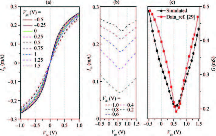
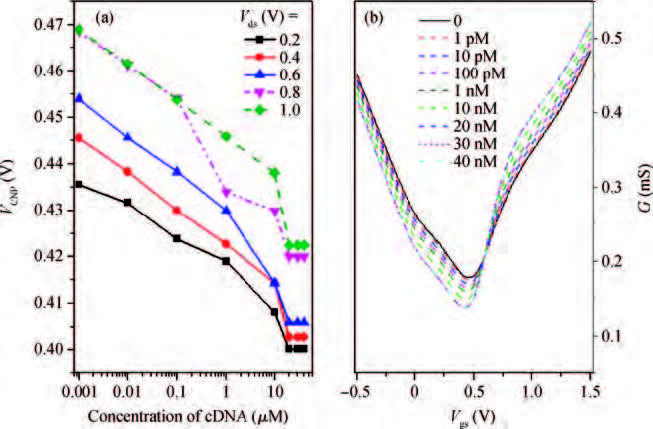
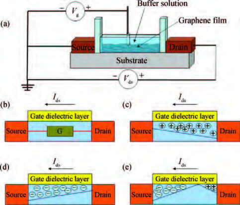
Processing math: 100%
J. Semicond. > 2016, Volume 37 > Issue 1 > 014005

SEMICONDUCTOR DEVICES

Sentaurus® based modeling and simulation for GFET's characteristic for ssDNA immobilization and hybridization

Yunfang Jia and Cheng Ju

+ Author Affiliations

 Corresponding author: Jia Yunfang,Email:

DOI: 10.1088/1674-4926/37/1/014005

PDF

Abstract: The graphene field effect transistor (GFET) has been widely studied and developed as sensors and functional devices. The first report about GFET sensing simulation on the device level is proposed. The GFET's characteristics, its responding for single strand DNA (ssDNA) and hybridization with the complimentary DNA (cDNA) are simulated based on Sentaurus, a popular CAD tool for electronic devices. The agreement between the simulated blank GFET feature and the reported experimental data suggests the feasibility of the presented simulation method. Then the simulations of ssDNA immobilization on GFET and hybridization with its cDNA are performed, the results are discussed based on the electron transfer (ET) mechanism between DNA and graphene.

Key words: graphene field effect transistorDNAsimulationelectron transferSentaurus

Graphene is a two-dimensional (2-D) sheet of sp2-bonded carbon atoms with a hexagonal configuration[1]. Due to its prominent and unique properties in eletronics,it is considered as an excellent nano-electronic material and a promising candidate for high speed transistors[2],energy storage[3],capacitors[4],and anodes in lithium ion batteries[5]. In the tremendous graphene related applications,the graphene field effect transistor (GFET) is only a little branch. However,it has provided an excellent platform for the detection of various biological and chemical agents[6, 7]. It was firstly published in 2009 on the discovery of GFET's high trans-conductance in an electrolyte solution and its dependence on the pH of the electrolyte[8]. Since then thousands of GFET-based bio-sensors have been developed. The absorbed protein molecules on graphene could be examined by the conductance's variations,which was enhanced by the increasing concentrations of BSA[8]. The hybridization of deoxyribonucleic acid (DNA) could be monitored by direct electrical detection based on GFET,and the resolution for the mismatched base was achieved as one base[9]. Not only bio-molecules but also bacteria and small inorganic chemicals could be specifically detected by these total electronic and solid-state sensing components. The detection of E.coli was realized with a sensitivity of 10 cfu/mL and high specificity[10]. Gas sensing could also be executed by solution gated GFET,and the lower limits for NH3 and CO2 were 30 and 4000 ppm,respectively[11]. Heavy metal ion (Hg2+) was discriminated and monitored in real time based on reduced graphene FET[12]. It has been demonstrated that this kind of GFET sensing platform was a quick sensing,label-free,portable and low-cost bio-electronic system,and it could be developed as a high throughput biochemical analyzer for environment monitoring,food supervising and drug screening.

DNA is a powerful bio-material. It has played an important role in biology,biochemistry and biophysics due to its function of carrying genetic information in all living species[13]. Lots of research has been carried out to prove that there are relationships between the electrical properties of DNA and its bio-physical structure when it undergoes replication,damage or repair[14]. Charge transfer along the molecules of DNA is an important micro-mechanism and it is reported to occur in diverse biological platforms[15]. Furthermore,as a natural nano-structure material,DNA has great potential applications in the field of molecule devices[16]. Zhu \textit{et al.} fabricated a DNA sensor based on thionine-graphene nano-composite (Th-G) and its detection limit could reach 1.26 × 10¹³ M (S/N = 3). With the rapid development of DNA related practical works,the systematical theory to explain the observed or reported phenomena is necessary. So,extensive theoretical studies and experiments were carried out,and it was proved that electron transfer (ET) can occur in the DNA molecule by two principal mechanisms[17, 18],which are "coherent transfer" and "thermal hopping". In a real DNA molecule,the dominant way in the process of ET will depend on its chain length[19].

The combination of DNA and GFET has given birth to a new kind of DNA sensors,called the aptamer sensor,in which single strand DNA (ssDNA) molecules are selected and grafted on the gate of a GFET[20, 21]. The applications of these DNA sensors are not only in the monitoring of DNA molecules,but also in the recognition of almost all chemical or biological analytes[22, 23, 24]. Lots of effort has been exerted on these GFETs based aptamer biochemical sensors recently. It has been verified by the published theoretical and experimental studies that in these sensing systems the interaction between ssDNA and graphene is the key point for understanding the responding of GFET[25]. For an electronic engineer,one is more concerned about its electronic performance and its capability of integrating with a modern electronic designing system. Currently,the experimental works or physical mechanisms' studies about GFET-DNA sensors could be extensively referred,but how to simulate their electronic behaviors in the environment of a general electronic designing system is relatively little. So,the emphasis of this work is put on the simulation of GFET-DNA sensors' electronic behaviors by Sentaurus\textregistered,which is a popular software for technology computer aided design (TCAD). This work provide a feasible method for the electronic simulation of GFET-DNA sensors,and it has good potential for achieving the TCAD of GFET-DNA sensors.

The structure of a common GFET-based biochemical sensor is depicted in Figure1(a). The explanation is outlined here. First,on the insulated substrate there is a rectangular graphene film,used as the conductive channel. Second,on the two ends of the channel there are two electrodes,called source and drain,respectively. Third,the gate electrode is above the graphene film and across a layer of buffer solution,used as the dielectric layer of the gate. Finally,the electrode of the source is grounded,which is the benchmark for the voltages applied by gate and drain. The voltages applied by gate and drain are named Vg and Vds,respectively. When there is an electric field along the conducting channel,the current between source and drain (Ids) will be formed. Based on Figure1(a),an analytic model for GFET is proposed and simulated based on Sentaurus\textregistered. The GFET Sentaurus simulation method is verified by comparing with the experimental data. Then the single strand DNA molecule's effects on GFET are simulated based on the proposed Sentaurus simulation method.

Figure  1.  (Color online) Schematics of device structure (a) and four working states (b, c, d, e). The bias voltage of three electrodes are defined in (a). There is no carriers’ accumulation or depletion in (b), the current of Ids is determined by the conductance of the graphene conducting channel itself (G). While in (c) and (d), one type of the carriers is depleted and the other is accumulated depending on the electric potential applied by the gate, where (c) is Vgs < 0 and (d) is Vgs > Vds > 0. Both accumulation and depletion happened when the relation of electric potential among three electrodes is Vds > Vgs > 0 (e).

It has been proved that the conductance of GFET could be modulated by Vg[1]. So the Ids could be modulated by Vg,when Vds is maintained as a constant value. With a given Vg,the arising and saturation value of Ids could be measured with the increasing of Vds. For GFET,no matter whether the positive or negative voltage of Vg is applied,the characteristic curves of Ids versus Vds could be observed and it is different from traditional Si based FET[26, 27, 28, 29, 30, 31]. The general explanation for GFET's bipolarity is accepted as: the carrier density and type in the channel can be modulated by the variation of Vg (the type of carriers could be electrons,holes or their coexistence)[32].

There were four working states when different voltages of Vg and Vds were applied on GFET[33, 34, 35]. As shown in Figures 1(b) to 1(e),the type of majority carriers in the graphene channel can be determined depending on Vg and Vds. When Vg was controlled at zero,there were no accumulated or depleted charges,as shown in Figure1(b). The carriers in the graphene conducting channel could be drifted by a positive electric field along the channel,then the drift current (Ids) is constructed. For Figure1(c),under the negative gate voltage (Vg < 0),holes are accumulated and electrons are depleted. The major carriers are holes in the channel of the GFET. When there is a positive electronic field from drain to source,Ids is formed. For Vg > Vds >~0,as shown in Figure1(d),the major carriers are accumulated electrons and Ids is formed by drifted electrons from source to drain. In the state of Vds > Vg > 0,there is a turning point in the channel as given in Figure1(e),which is called the offset point. From this point to drain,electrons are depleted and holes are accumulated. It is opposite from the turning point to source. In this situation,electrons and holes are drifted oppositely to form the current Ids.

The DNA molecules are a kind of biological macromolecules built from repeating sugar molecules and phosphate groups. Each sugar group is attached to one of the four bases,which are guanine (G),cytosine (C),adenine (A) and thymine (T). The negative charge of phosphate groups make single- and double-strand DNA negatively charged. Double-strand DNA (dsDNA) consists of two strands of DNA around each other and hydrogen bonds between the bases coupling the two strands together. The dsDNA is more negatively charged than the ssDNA since the amount of phosphate groups in the dsDNA is higher than in the ssDNA. The experimental and theoretical works have been carried out and led to substantial clarification of the charge-transfer mechanism in DNA[36, 37, 38, 39]. The dominant mechanism falls into two ways[19, 40]: one way is that the charge can transfer from the donor to the acceptor groups by the tunnel effect,and the charge-transfer rate will sharply decrease with the length of the DNA molecule chain increasing; the other way is that the charge can transfer by "hopping" from a base pair to another,and in this case the charge-transfer rate is weakly dependent on the distance between donor and acceptor groups. Moreover,the process of charge transfer in DNA molecules could be affected by many factors including the length of DNA molecules,the sequence of base pairs,the internal energy of donor and acceptor,the ambient environment temperature and so on[18, 41].

Due to a high surface area,graphene has a strong biocompatibility[42, 43, 44]. There is an interaction (π-π) between DNA molecules and the surface of graphene which results in a remarkable influence on the carriers' density of the GFET by transferring electrons from the DNA to the graphene film. Then the channel conductance of the GFET can be affected consequently[45]. It means that the channel conductance of the GFET will be affected by changing the density of DNA molecules immobilized on the surface of the graphene channel[46]. So it is a reasonable inference that Ids will change when ssDNA is immobilized on the gate surface of GFET and Vds and Vgs. Furthermore,since there are more charges on the molecules of dsDNA than ssDNA,and ET in the structure of dsDNA is more easier than in ssDNA[19],another speculation could be formed that more electrons will transfer from dsDNA to graphene film when immobilized ssDNA molecules are hybridized with its complementary partner.

There are a large number of physical analytical models in Sentaurus. It is a popular CAD tool in micro-electronic devices' design[47, 48]. Graphene is a novel nanomaterial and its parameters of properties need to be defined in Sentaurus,such as the effective mass of electron and hole,mobility at room temperature and band gap[49]. In the environment of Sentaurus,GFET is modelled firstly and its sensing for ssDNA immobilization and the following hybridization are simulated. The modelling method is outlined here.

Since the conducting channel of GFET is graphene,the concentration of carriers in the intrinsic semiconductor is summarized as:

ni(T)=NC(T)NV(T)exp[Eg(T)2kT],

(1)

where T is the lattice temperature,Eg(T) is the energy of the band gap,k is Boltzmann factors,Nc(T) and Nv(T) are the effective density-of-state (DOS) for electrons and holes,respectively. The forms and parameter values of Eg(T), Nc(T) and Nv(T) are listed in Table1.

Table  1.  The best values for the correlation coefficients A,B and C.
DownLoad: CSV  | Show Table

By default,a "band gap narrowing" model is activated with the Bennett Wilson model. Since in the process of simulation,graphene has been undoped,the Bennett Wilson model needs to be turned off. Graphene possesses a stable structure without atomic defects; even if under the action of an external force,the arrangement of carbon atoms is not changed. The carriers of graphene move on their own orbit,they are not affected by lattice defects. Thus the constant mobility model is selected in the process of simulation and defined as:

uconst=uL(T300K)λ,

(2)

where uL = 5000 cm2/(Vs) is the mobility due to bulk photon scattering,λ =1 is a correlation index.

The model for DNA detection was proposed by HKF Abadi[50]:

Id=3q2(3πd3t3kBT)0.5hL[J0.5(η)+J0.5(η)]×αFVgs,

(3)

where q is the electron charge,d= 1.42 {\AA} is the length of carbon-carbon (C-C) bond,t= 2.7 eV is the nearest neighbour C-C tight binding overlap energy,kB is the Boltzmann's constant and L shows the length of the conducting channel. Furthermore,j0.5(η) and j0.5(η) are the Fermi-Dirac integral of orders 0.5 whose value can numerically be solved by employing the partial integration method. α is the DNA sensing factor and different concentrations of DNA molecules are expressed in the form of the F parameter. The relationship between α and F is a quadratic function as:

α=AF2+BF+C,

(4)

where A= 13,B= 50 and C= 4070 are the correlation coefficient between α and F. Thus,based on the electrical mechanism of DNA molecules and Equation (3),the current-voltage model of GFET for DNA detection can be simplified as:

Id=MαFVgs,

(5)

where M is a parameter as the representation of GFET properties and its specific form is equal to the different part between Equations (3) and (5). This model is reliable for graphene-based DNA sensors,since the values of the parameters A,B and C in Equation (4) are calculated based on trial and error.

In this section,the simulation for GFET was executed and compared with experimental data,firstly. Then,GFET responding for ssDNA immobilization and hybridization with complimentary ssDNA was simulated in the next two subsections.

First,volt-ampere characteristic curves under different Vgs and the transfer characteristic curves under different Vds were shown in Figures 2(a) and 2(b),respectively. It was exhibited that the slopes of the I-V characteristic curves in Figure2(a) were varied by Vgs. When Vgs was varied negatively from 0.75 to 0.5,the curves stood up gradually. It means when the gate is more negatively powered more holes will be accumulated in the conducting channel,then the I-V curves' slopes will be increased. While being positively varied Vgs from 0.75 to 1.5 will make more electrons accumulated and holes depleted,which means Ids will be increased at the same Vds,as given in Figure2(a). That is to say,at the constant Vds,increased Ids could be got when Vgs is varied in two directions,as shown in Figure2(b) which is one of the typical bipolar characteristic curves of GFET.

Figure  2.  (Color online) (a) Current–voltage characteristic of GFET in a different value of the Vgs. (b) Transfer characteristic of GFET in a different value of the Vds. (c) Comparison between the conductance of the GFET model with experimental data.

The other of the GFET's bipolar feature could be expressed in the channel's conductance (G) versus Vgs. The value of G is defined in Equation (6):

G=IdsVds|Vgs.

(6)

Herein the values of G were calculated and plotted in Figure2(c). The operating mechanism of the field-effect transistor given in Section 2.2 implies that major carriers can be tuned continuously between holes and electrons by Vgs. So there should be a Vgs-depended conductance (G),as given in Figure2(c). From the G-Vgs curves it could be identified clearly that the turning point exists in both experimental data[29] and our simulated result. This point is called the charge neutrality point (CNP). The appearance of the CNP is in accordance with the one of the working state,which is given in Section 2.2,Figure1(e). At this point,the channel conductance of the GFET is the lowest. The simulated results were compared with the experimental results from reference[29]. There is a good agreement between the simulated results and the experimental data in the reference. So it is believed that the proposed model is reasonable.

DNA is an electron-rich molecule. When the ssDNA molecules are covalently grafted on graphene,the number of carriers will be changed in graphene so as to induce the variation of its conductance. For GFET,this chain reaction is expressed as the fluctuation of Ids. The simulation of ssDNA modified GFET provides an opportunity to examine GFET's responding and gives assistance to have an optimal working condition for the detection of target ssDNA.

The simulations of GFET's responding for ssDNA immobilization and hybridization were executed according to Equations (3),(4) and (5). The effects of ssDNA concentration on the transferring characteristic curves could be observed in Figures 3(a) to 3(c) for Vds = 0.2,0.6,1.0,respectively. The moving of CNP accompanying the increasing of ssDNA concentrations is obvious for the three plots in Figure3. The changing tendency of CNP and its relation with ssDNA concentration is extracted and plotted in Figure4(a).

Figure  3.  (Color online) The effects of ssDNA binding on GFET’s transferring characteristics when Vds is constant at (a) 0.2 V, (b) 0.6 V and (c) 1.0 V.
Figure  4.  (Color online) The effects of immobilizing different concentrations of ssDNA on (a) the variation of GFET’s CNP and (b) the conductance.

In Figure3(a) the decrease of Ids with the increase of ssDNA concentration could be identified clearly on the left side of the CNP at the same Vgs. This could be explained that ET from DNA to graphene neutralize some of the accumulated-state holes (as shown in Figure2(c)). The amount of major carriers is decreased so that the current along the channel is decreased. On the right side of the CNP,the shifting of Ids is upward when Vgs is constant. It is also coincident with ET theory. While there are differences among Figures 3(a),3(b) and 3(c),when Vds is lower (0.2 V in Figure3(a)),the value of Ids at the CNP is decreased directly with the left moving of the CNP; but in the other two plots,the variations of Ids at the CNP are not in a single direction,they increase firstly,then decrease. This turning sight is more obvious when Vds increases from 0.6 to 1.0 V,as shown in Figures 3(b) and 3(c). In general,the voltages of the CNP (VCNP) are lowered with the growing of ssDNA concentrations almost linearly and saturated at 20 μM. In this figure,the influences of Vds are relatively small,that means the CNP could be developed as an indicator for DNA sensing.

At the same time,the channel conductance G (defined in Equation (6)) is extracted by the same method as the one given in Section 3.1 and plotted in Figure4(b) based on the simulation of I-V characteristics (which is very similar to Figure2(a) and omitted here). The curves of G-Vgs in different ssDNA concentrations exhibit a similar bipolar feature as in Figure2(c). The influences of ssDNA immobilization are expressed on the left downward moving of the curves. It is in coincidence with the ET mechanism,which was discussed in the last paragraph.

The dsDNA comes into being when the immobilized ssDNA hybridize with its complimentary ssDNA (cDNA). Since there are more charges in the chain of dsDNA than ssDNA,the electric features of GFET will be modified further. In this section it mainly concerns the effect of hybridized ssDNA's concentrations on the transferring characteristics of hybridized dsDNA-GFET,which is presented in Figures 5(a),5(b) and 5(c) when Vds is constant at 0.2,0.6 and 1.0 V,respectively. The simulation is conducted by choosing GFET's responding of 20 μM ssDNA as control,i.e. 0 pM in Figure5. The concentrations of cDNA are arranged from 1 pM to 40 nM. Discussions for Figure5 are presented at here.

Figure  5.  (Color online) Simulation of transferring characteristics after being hybridized with complimentary ssDNA, the concentrations of which are 0 to 40 nM, and the drain–source voltage is controlled at (a) 0.2 V, (b) 0.6 V and (c) 1.0 V.

First,the shapes of the curves in three plots are very similar,the arising of Vds causes the upward shift of the whole curves. That means there is no offset point (defined in Section 2.2) in the three situations. Ids is constructed by the drift of one kind of majorities. When compared with Figure3,it could be found that at the CNP,Ids are lowered without fluctuations as in Figure3. The deduction is also presented as ET theory. Because there are so many electrons injected by DNA molecules which are immobilized or hybridized on the GFET that the increasing of Vds does not cause the appearance of the offset point in the channel. The working states of the dsDNA-GFET are switched between holes' accumulation and electrons' accumulation as depicted in Section 2.2.

Second,there are still points of intersection in Figures 5(a),5(b) and 5(c),respectively. On the left of this point,Ids decreases with the increasing of cDNA concentration when Vgs is constant,while on the right of it,Ids varies in an opposite way. It is deduced that when Vgs is lower than this points' x-coordinate the GFET is gated more negatively,the working state falls into Figure2(c) and the majorities are holes. So,more electrons are injected from cDNA,more holes will be shielded,and Ids will decrease. While the situations of Vgs exceed the point of intersection,the electrons are accumulated as depicted in Figure2(d); the injected electrons will enhance the amount of major carriers,which is just in accordance with the increased Ids (on the right of the intersection points) in Figure5.

Finally,the VCNP and channel conductance G are extracted and plotted in Figures 6(a) and 6(b). When compared with Figure4(a),there are relatively small variations of VCNP. The reason is deduced as: the injected electrons from ssDNA enhance the amounts of electrons in GFET and make the neutralization of holes easier; so the VCNP for dsDNA-GFET are relatively smaller than ssDNA-GFET. The channel conductance of dsDNA-GFET is extracted in the same way as described in Section 3.1. The ET mechanism between the DNA molecule and graphene is still applicable. Induced electrons screen the accumulated holes when Vgs is on the left of the intersecting point so the conductance is lowered with the increasing of cDNA; while for the right of this point,G is increased by the electrons donated by hybridized cDNA.

Figure  6.  (Color online) The effects of hybridized cDNA on (a) the variation of GFET’s CNP and (b) the conductance.

Based on a popular CAD tool for electric devices,GFET is simulated and compared with the reported experimental data; simulation of ssDNA immobilization on GFET and the hybridization with its cDNA are also performed and discussed based on the ET mechanism of the DNA molecule and between DNA and graphene. The agreement between the simulated results and the experimental data indicates the feasibility of the presented simulation method. The simulated results for ssDNA immobilizing and cDNA hybridizing are also coincident with ET mechanisms. It is believed that the presented method for the simulation of GFET and DNA sensing would be helpful for electronic researchers to understand this kind of biosensor behavior before experiments,and it would be a cost-efficient way for bioelectroinc sensing system design.


[1]
[2]
[3]
[4]
[5]
[6]
[7]
[8]
[9]
[10]
[11]
[12]
[13]
[14]
[15]
[16]
[17]
[18]
[19]
[20]
[21]
[22]
[23]
[24]
[25]
[26]
[27]
[28]
[29]
[30]
[31]
[32]
[33]
[34]
[35]
[36]
[37]
[38]
[39]
[40]
[41]
[42]
[43]
[44]
[45]
[46]
[47]
[48]
[49]
[50]
Fig. 1.  (Color online) Schematics of device structure (a) and four working states (b, c, d, e). The bias voltage of three electrodes are defined in (a). There is no carriers’ accumulation or depletion in (b), the current of Ids is determined by the conductance of the graphene conducting channel itself (G). While in (c) and (d), one type of the carriers is depleted and the other is accumulated depending on the electric potential applied by the gate, where (c) is Vgs < 0 and (d) is Vgs > Vds > 0. Both accumulation and depletion happened when the relation of electric potential among three electrodes is Vds > Vgs > 0 (e).

Fig. 2.  (Color online) (a) Current–voltage characteristic of GFET in a different value of the Vgs. (b) Transfer characteristic of GFET in a different value of the Vds. (c) Comparison between the conductance of the GFET model with experimental data.

Fig. 3.  (Color online) The effects of ssDNA binding on GFET’s transferring characteristics when Vds is constant at (a) 0.2 V, (b) 0.6 V and (c) 1.0 V.

Fig. 4.  (Color online) The effects of immobilizing different concentrations of ssDNA on (a) the variation of GFET’s CNP and (b) the conductance.

Fig. 5.  (Color online) Simulation of transferring characteristics after being hybridized with complimentary ssDNA, the concentrations of which are 0 to 40 nM, and the drain–source voltage is controlled at (a) 0.2 V, (b) 0.6 V and (c) 1.0 V.

Fig. 6.  (Color online) The effects of hybridized cDNA on (a) the variation of GFET’s CNP and (b) the conductance.

Table 1.   The best values for the correlation coefficients A,B and C.

DownLoad: CSV
[1]
[2]
[3]
[4]
[5]
[6]
[7]
[8]
[9]
[10]
[11]
[12]
[13]
[14]
[15]
[16]
[17]
[18]
[19]
[20]
[21]
[22]
[23]
[24]
[25]
[26]
[27]
[28]
[29]
[30]
[31]
[32]
[33]
[34]
[35]
[36]
[37]
[38]
[39]
[40]
[41]
[42]
[43]
[44]
[45]
[46]
[47]
[48]
[49]
[50]
1

Perylene diimide self-assembly: From electronic structural modulation to photocatalytic applications

Weiqin Wei, Shuxin Ouyang, Tierui Zhang

Journal of Semiconductors, 2020, 41(9): 091708. doi: 10.1088/1674-4926/41/9/091708

2

Simulation and application of external quantum efficiency of solar cells based on spectroscopy

Guanlin Chen, Can Han, Lingling Yan, Yuelong Li, Ying Zhao, et al.

Journal of Semiconductors, 2019, 40(12): 122701. doi: 10.1088/1674-4926/40/12/122701

3

Engineering in-plane silicon nanowire springs for highly stretchable electronics

Zhaoguo Xue, Taige Dong, Zhimin Zhu, Yaolong Zhao, Ying Sun, et al.

Journal of Semiconductors, 2018, 39(1): 011001. doi: 10.1088/1674-4926/39/1/011001

4

Simulation approach for optimization of ZnO/c-WSe2 heterojunction solar cells

Shihua Huang, Qiannan Li, Dan Chi, Xiuqing Meng, Lü He, et al.

Journal of Semiconductors, 2017, 38(4): 044008. doi: 10.1088/1674-4926/38/4/044008

5

Study of the effect of switching speed of the a-SiC/c-Si (p)-based, thyristor-like, ultra-high-speed switches, using two-dimensional simulation techniques

Evangelos I. Dimitriadis, Nikolaos Georgoulas

Journal of Semiconductors, 2017, 38(5): 054001. doi: 10.1088/1674-4926/38/5/054001

6

Simulation of double junction In0.46Ga0.54N/Si tandem solar cell

M. Benaicha, L. Dehimi, Nouredine Sengouga

Journal of Semiconductors, 2017, 38(4): 044002. doi: 10.1088/1674-4926/38/4/044002

7

Simulation of a high-efficiency silicon-based heterojunction solar cell

Jian Liu, Shihua Huang, Lü He

Journal of Semiconductors, 2015, 36(4): 044010. doi: 10.1088/1674-4926/36/4/044010

8

Modeling and simulation of single-event effect in CMOS circuit

Suge Yue, Xiaolin Zhang, Yuanfu Zhao, Lin Liu

Journal of Semiconductors, 2015, 36(11): 111002. doi: 10.1088/1674-4926/36/11/111002

9

Analytical modeling and simulation of germanium single gate silicon on insulator TFET

T. S. Arun Samuel, N. B. Balamurugan

Journal of Semiconductors, 2014, 35(3): 034002. doi: 10.1088/1674-4926/35/3/034002

10

The influence of the channel electric field distribution on the polarization Coulomb field scattering in AlN/GaN heterostructure field-effect transistors

Yingxia Yu, Zhaojun Lin, Yuanjie Lü, Zhihong Feng, Chongbiao Luan, et al.

Journal of Semiconductors, 2014, 35(12): 124007. doi: 10.1088/1674-4926/35/12/124007

11

Simulation of through via bottom-up copper plating with accelerator for the filling of TSVs

Heng Wu, Zhen'an Tang, Zhu Wang, Wan Cheng, Daquan Yu, et al.

Journal of Semiconductors, 2013, 34(9): 096001. doi: 10.1088/1674-4926/34/9/096001

12

Structural parameters improvement of an integrated HBT in a cascode configuration opto-electronic mixer

Hassan Kaatuzian, Hadi Dehghan Nayeri, Masoud Ataei, Ashkan Zandi

Journal of Semiconductors, 2013, 34(9): 094001. doi: 10.1088/1674-4926/34/9/094001

13

Simulation study on short channel double-gate junctionless field-effect transistors

Meile Wu, Xiaoshi Jin, Rongyan Chuai, Xi Liu, Jong-Ho Lee, et al.

Journal of Semiconductors, 2013, 34(3): 034004. doi: 10.1088/1674-4926/34/3/034004

14

A simulation of doping and trap effects on the spectral response of AlGaN ultraviolet detectors

Sidi Ould Saad Hamady

Journal of Semiconductors, 2012, 33(3): 034002. doi: 10.1088/1674-4926/33/3/034002

15

Fabrication and photoelectrical characteristics of ZnO nanowire field-effect transistors

Fu Xiaojun, Zhang Haiying, Guo Changxin, Xu Jingbo, Li Ming, et al.

Journal of Semiconductors, 2009, 30(8): 084002. doi: 10.1088/1674-4926/30/8/084002

16

A novel GAAC FinFET transistor: device analysis, 3D TCAD simulation, and fabrication

Xiao Deyuan, Wang Xi, Yuan Haijiang, Yu Yuehui, Xie Zhifeng, et al.

Journal of Semiconductors, 2009, 30(1): 014001. doi: 10.1088/1674-4926/30/1/014001

17

Two-Dimensional Static Numerical Modeling and Simulation of AlGaN/GaN HEMT

Xue Lijun, Xia Yang, Liu Ming, Wang Yan, Shao Xue, et al.

Chinese Journal of Semiconductors , 2006, 27(2): 298-303.

18

Photolithography Process Simulation for Integrated Circuitsand Microelectromechanical System Fabrication

Zhou Zaifa, Huang Qing'an, Li Weihua

Chinese Journal of Semiconductors , 2006, 27(4): 705-711.

19

Effect of Relaxation Time on Electron Transport Properties in Double-Barrier Structures

Dai Zhenhong, Ni Jun

Chinese Journal of Semiconductors , 2006, 27(4): 604-608.

20

Full Band Monte Carlo Simulation of Electron Transport in Ge with Anisotropic Scattering Process

Chen, Yong, and, Ravaioli, Umberto, et al.

Chinese Journal of Semiconductors , 2005, 26(3): 465-471.

  • Search

    Advanced Search >>

    GET CITATION

    Yunfang Jia, Cheng Ju. Sentaurus® based modeling and simulation for GFET's characteristic for ssDNA immobilization and hybridization[J]. Journal of Semiconductors, 2016, 37(1): 014005. doi: 10.1088/1674-4926/37/1/014005
    Y F Jia, C Ju. Sentaurus® based modeling and simulation for GFET\'s characteristic for ssDNA immobilization and hybridization[J]. J. Semicond., 2016, 37(1): 014005. doi: 10.1088/1674-4926/37/1/014005.
    shu

    Export: BibTex EndNote

    Article Metrics

    Article views: 3039 Times PDF downloads: 51 Times Cited by: 0 Times

    History

    Received: 19 April 2015 Revised: Online: Published: 01 January 2016

    Catalog

      Email This Article

      User name:
      Email:*请输入正确邮箱
      Code:*验证码错误
      Yunfang Jia, Cheng Ju. Sentaurus® based modeling and simulation for GFET's characteristic for ssDNA immobilization and hybridization[J]. Journal of Semiconductors, 2016, 37(1): 014005. doi: 10.1088/1674-4926/37/1/014005 ****Y F Jia, C Ju. Sentaurus® based modeling and simulation for GFET\'s characteristic for ssDNA immobilization and hybridization[J]. J. Semicond., 2016, 37(1): 014005. doi: 10.1088/1674-4926/37/1/014005.
      Citation:
      Yunfang Jia, Cheng Ju. Sentaurus® based modeling and simulation for GFET's characteristic for ssDNA immobilization and hybridization[J]. Journal of Semiconductors, 2016, 37(1): 014005. doi: 10.1088/1674-4926/37/1/014005 ****
      Y F Jia, C Ju. Sentaurus® based modeling and simulation for GFET\'s characteristic for ssDNA immobilization and hybridization[J]. J. Semicond., 2016, 37(1): 014005. doi: 10.1088/1674-4926/37/1/014005.

      Sentaurus® based modeling and simulation for GFET's characteristic for ssDNA immobilization and hybridization

      DOI: 10.1088/1674-4926/37/1/014005
      Funds:

      Project supported by the National Natural Science Foundation of China (No. 61371028) and the Tianjin Natural Science Foundation (No. 12JCZDJC22400).

      More Information

      Catalog

        /

        DownLoad:  Full-Size Img  PowerPoint
        Return
        Return